- 您现在的位置:买卖IC网 > PDF目录16617 > DC1018B-B (Linear Technology)DEMO BOARD FOR LT4356-2 PDF资料下载
参数资料
| 型号: | DC1018B-B |
| 厂商: | Linear Technology |
| 文件页数: | 14/26页 |
| 文件大小: | 0K |
| 描述: | DEMO BOARD FOR LT4356-2 |
| 设计资源: | DC1018B Design File DC1018B Schematic |
| 标准包装: | 1 |
| 主要目的: | 过压防护 |
| 嵌入式: | 否 |
| 已用 IC / 零件: | LT4356-2 |
| 已供物品: | 板 |
| 相关产品: | LT4356HDE-3-ND - IC REG OVP FAULT TIMER 12DFN LT4356HS-3#PBF-ND - IC REG OVP W/LATCHOFF 16SOIC LT4356HMS-3#PBF-ND - IC REG OVP W/LATCHOFF 10-MSOP LT4356HDE-3#PBF-ND - IC REG OVP W/LATCHOFF 12DFN LT4356HS-3#TRPBF-ND - IC REG OVP FAULT TIMER 16SOIC LT4356HMS-3#TRPBF-ND - IC REG OVP FAULT TIMER 10MSOP LT4356HDE-3#TRPBF-ND - IC REG OVP FAULT TIMER 12DFN LT4356MPS-2#TRPBF-ND - IC SURGE STOPPER ADJ 16-SOIC LT4356MPS-1#TRPBF-ND - IC SURGE STOPPER ADJ 16-SOIC LT4356MPMS-1#TRPBF-ND - IC SURGE STOPPER ADJ 10-MSOP 更多... |
�� �
�
�LT4356-1/LT4356-2�
�APPLICATIONS� INFORMATION�
�MOSFET� stress� is� the� result� of� power� dissipated� within�
�the� device.� For� long� duration� surges� of� 100ms� or� more,�
�stress� is� increasingly� dominated� by� heat� transfer;� this� is�
�a� matter� of� device� packaging� and� mounting,� and� heatsink�
�thermal� mass.� This� is� analyzed� by� simulation,� using� the�
�V� REG�
�V� PK�
�MOSFET� thermal� model.�
�V� IN�
�t� r�
�I� LOAD� 2� (� V� PK� –� V� REG� )� τ�
�P� 2� t� =�
�(W� 2� s)�
�?� 1� (� b� ?� a� )� 3� 1� ?� b� ?� ?�
�?� ?�
�P� 2� t� =� I� LOAD� 2� ?� tr� +� τ� ?� 2a� 2� ln� +� 3a� 2� +� b� 2� ?� 4ab� ?� ?�
�?� ?� 3�
�?�
�Forshortdurationtransientsoflessthan100ms,MOSFET�
�survival� is� increasingly� a� matter� of� safe� operating� area�
�(SOA),� an� intrinsic� property� of� the� MOSFET.� SOA� quanti-�
�?es� the� time� required� at� any� given� condition� of� V� DS� and�
�I� D� to� raise� the� junction� temperature� of� the� MOSFET� to� its�
�rated� maximum.� MOSFET� SOA� is� expressed� in� units� of�
�watt-squared-seconds� (P� 2� t).� This� ?gure� is� essentially� con-�
�stant� for� intervals� of� less� than� 100ms� for� any� given� device�
�type,� and� rises� to� in?nity� under� DC� operating� conditions.�
�Destruction� mechanisms� other� than� bulk� die� temperature�
�distort� the� lines� of� an� accurately� drawn� SOA� graph� so� that�
�P� 2� t� is� not� the� same� for� all� combinations� of� I� D� and� V� DS� .�
�In� particular� P� 2� t� tends� to� degrade� as� V� DS� approaches� the�
�maximum� rating,� rendering� some� devices� useless� for�
�absorbing� energy� above� a� certain� voltage.�
�Calculating� Transient� Stress�
�To� select� a� MOSFET� suitable� for� any� given� application,� the�
�SOA� stress� must� be� calculated� for� each� input� transient�
�which� shall� not� interrupt� operation.� It� is� then� a� simple� matter�
�to� chose� a� device� which� has� adequate� SOA� to� survive� the�
�maximum� calculated� stress.� P� 2� t� for� a� prototypical� transient�
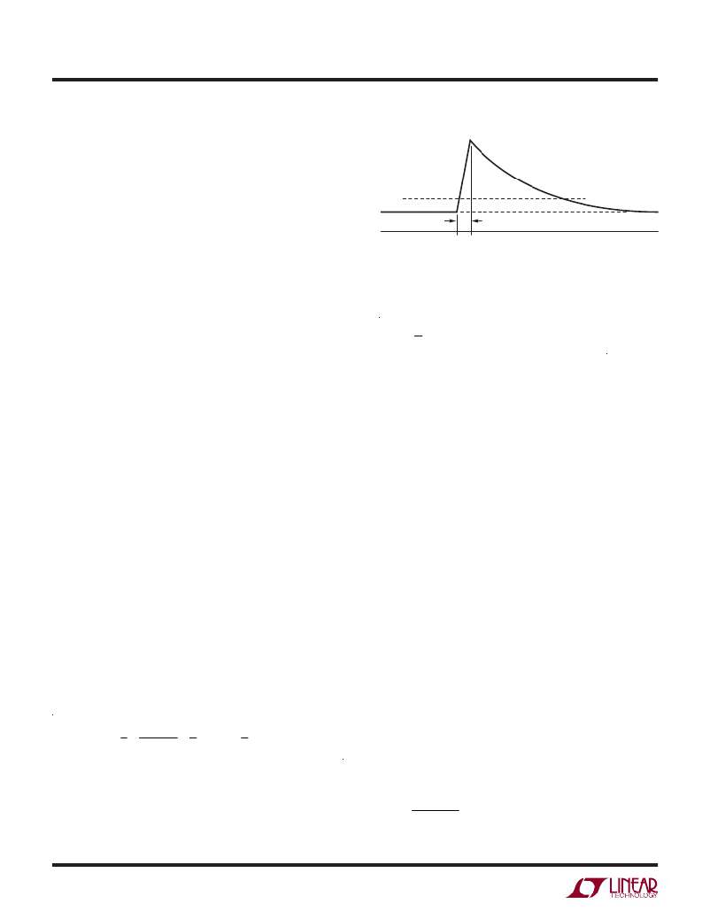
�waveform� is� calculated� as� follows� (Figure� 4).�
�Let�
�a� =� V� REG� –� V� IN�
�b� =� V� PK� –� V� IN�
�(V� IN� =� Nominal� Input� Voltage)�
�Then�
�b� 2� ?� a�
�4356� F04�
�Figure� 4.� Safe� Operating� Area� Required� to� Survive� Prototypical�
�Transient� Waveform�
�Typically� V� REG� ≈� V� IN� and� τ� >>� t� r� simplifying� the� above� to�
�1� 2�
�2�
�For� the� transient� conditions� of� V� PK� =� 80V,� V� IN� =� 12V,� V� REG�
�=� 16V,� t� r� =� 10μs� and� τ� =� 1ms,� and� a� load� current� of� 3A,� P� 2� t�
�is� 18.4W� 2� s—easily� handled� by� a� MOSFET� in� a� D-pak� pack-�
�age.� The� P� 2� t� of� other� transient� waveshapes� is� evaluated� by�
�integrating� the� square� of� MOSFET� power� versus� time.�
�Calculating� Short-Circuit� Stress�
�SOA� stress� must� also� be� calculated� for� short-circuit� condi-�
�tions.� Short-circuit� P� 2� t� is� given� by:�
�P� 2� t� =� (V� IN� ?� Δ� V� SNS� /R� SNS� )� 2� ?� t� TMR� (W� 2� s)�
�where,� Δ� V� SNS� is� the� SENSE� pin� threshold,� and� t� TMR� is� the�
�overcurrent� timer� interval.�
�For� V� IN� =� 14.7V,� V� SNS� =� 50mV,� R� SNS� =� 12m� Ω� and� C� TMR�
�=� 100nF,� P� 2� t� is� 6.6W� 2� s—less� than� the� transient� SOA�
�calculated� in� the� previous� example.� Nevertheless,� to�
�account� for� circuit� tolerances� this� ?gure� should� be� doubled�
�to� 13.2W� 2� s.�
�Limiting� Inrush� Current� and� GATE� Pin� Compensation�
�The� LT4356� limits� the� inrush� current� to� any� load� capacitance�
�by� controlling� the� GATE� pin� voltage� slew� rate.� An� external�
�capacitor� can� be� connected� from� GATE� to� ground� to� slow�
�down� the� inrush� current� further� at� the� expense� of� slower�
�turn-off� time.� The� gate� capacitor� is� set� at:�
�C1� =�
�I� GATE(UP)�
�I� INRUSH�
�?C� L�
�4356fa�
�14�
�相关PDF资料 |
PDF描述 |
|---|---|
| L-07C56NJV6T | CER INDUCTOR 56NH 0402 |
| L-07C43NJV6T | CER INDUCTOR 43NH 0402 |
| L-05B5N6KV6T | CER INDUCTOR 5.6NH 0201 |
| L-05B5N1KV6T | CER INDUCTOR 5.1NH 0201 |
| H3AKH-2606G | IDC CABLE - HSC26H/AE26G/HPK26H |
相关代理商/技术参数 |
参数描述 |
|---|---|
| DC1018B-C | 功能描述:DEMO BOARD FOR LT4356-3 RoHS:否 类别:编程器,开发系统 >> 评估演示板和套件 系列:- 标准包装:1 系列:- 主要目的:数字电位器 嵌入式:- 已用 IC / 零件:AD5258 主要属性:- 次要属性:- 已供物品:板 相关产品:AD5258BRMZ1-ND - IC POT DGTL I2C1K 64P 10MSOPAD5258BRMZ10-ND - IC POT DGTL I2C 10K 64P 10MSOPAD5258BRMZ100-ND - IC POT DGTL I2C 100K 64P 10MSOPAD5258BRMZ50-ND - IC POT DGTL I2C 50K 64P 10MSOPAD5258BRMZ1-R7-ND - IC POT DGTL I2C 1K 64P 10MSOPAD5258BRMZ10-R7-ND - IC POT DGTL I2C 10K 64P 10MSOPAD5258BRMZ50-R7-ND - IC POT DGTL I2C 50K 64P 10MSOPAD5258BRMZ100-R7-ND - IC POT DGTL I2C 100K 64P 10MSOP |
| DC101-BB-B | 制造商:Carling Technologies 功能描述:D-SERIES TOGGLE SWITCH - Bulk |
| DC101-PB-B | 制造商:Carling Technologies 功能描述:D-SERIES TOGGLE SWITCH - Bulk |
| DC101-PB-B/728-15907 | 制造商:Carling Technologies 功能描述:D-SERIES TOGGLE SWITCH - Bulk |
| DC101-PB-B-XTH1 | 制造商:Carling Technologies 功能描述:D-SERIES TOGGLE SWITCH - Bulk |
发布紧急采购,3分钟左右您将得到回复。