- 您现在的位置:买卖IC网 > PDF目录17033 > DC1067A-B (Linear Technology)BOARD DELTA SIGMA ADC LTC2450-1 PDF资料下载
参数资料
| 型号: | DC1067A-B |
| 厂商: | Linear Technology |
| 文件页数: | 6/20页 |
| 文件大小: | 0K |
| 描述: | BOARD DELTA SIGMA ADC LTC2450-1 |
| 软件下载: | QuikEval System |
| 设计资源: | DC1067A Design File DC1067A Schematic |
| 标准包装: | 1 |
| 系列: | QuikEval™ |
| ADC 的数量: | 1 |
| 位数: | 16 |
| 采样率(每秒): | 30 |
| 数据接口: | 串行,SPI? |
| 已用 IC / 零件: | LTC2450-1 |
| 已供物品: | 板 |
| 相关产品: | LTC2450IDC#TRPBF-ND - IC ADC 16BIT DELTA SIG 6-DFN LTC2450IDC-1#TRPBF-ND - IC ADC 16BIT DELTA SIG 6-DFN LTC2450IDC-1#TRMPBFTR-ND - IC ADC 16BIT DELTA SIG 6-DFN LTC2450IDC#TRMPBFTR-ND - IC ADC 16BIT DELTA SIG 6-DFN LTC2450CDC-1#TRPBF-ND - IC ADC 16BIT DELTA SIG 6-DFN LTC2450CDC-1#TRMPBFTR-ND - IC ADC 16BIT DELTA SIG 6-DFN LTC2450CDC#TRPBF-ND - IC ADC 16BIT DELTA SIG 6-DFN LTC2450CDC#TRMPBFTR-ND - IC ADC 16BIT DELTA SIG 6-DFN |
LTC2450
14
2450fb
APPLICATIONS INFORMATION
Digital Signal Levels
The LTC2450’s digital interface is easy to use. Its digital
inputs (SCK and CS) accept standard CMOS logic levels
and the internal hysteresis receivers can tolerate edge
rates as slow as 100μs. However, some considerations
are required to take advantage of the exceptional accuracy
and low supply current of this converter.
The digital output signal SDO is less of a concern because
it is not active during the conversion cycle.
While a digital input signal is in the range 0.5V to VCC
–0.5V, the CMOS input receiver may draw additional
current from the power supply. Due to the nature of CMOS
logic, a slow transition within this voltage range may cause
an increase in the power supply current drawn by the
converter, particularly in the low power operation mode
within the SLEEP state. Thus, for low power consumption
it is highly desirable to provide relatively fast edges for the
two digital input pins SCK and CS, and to keep the digital
input logic levels at VCC or GND.
At the same time, during the CONVERT state, undershoot
and/or overshoot of fast digital signals connected to the
LTC2450 pins may alter the conversion result. Under-
shoot and overshoot can occur because of an impedance
mismatch at the converter pin combined with very fast
transition times. This problem becomes particularly difcult
when shared control lines are used and multiple reec-
tions may occur. The solution is to carefully terminate all
transmission lines close to their characteristic impedance.
Parallel termination is seldom an acceptable option in low
power systems so a series resistor between 27Ω and 56Ω
placed near the driver may eliminate this problem. The
actual resistor value depends upon the trace impedance
and connection topology. An alternate solution is to reduce
the edge rate of the control signals, keeping in mind the
concerns regarding slow edges mentioned above.
Particular attention should be given to congurations in
which a continuous clock signal is applied to SCK pin during
the CONVERT state. While LTC2450 will ignore this signal
from a logic point of view the signal edges may create
unexpected errors depending upon the relation between
its frequency and the internal oscillator frequency. In such
a situation it is benecial to use edge rates of about 10ns
and to limit potential undershoot to less than 0.3V below
GND and overshoot to less than 0.3V above VCC.
Noisy external circuitry can potentially impact the output
under 2-wire operation. In particular, it is possible to get
the LTC2450 into an unknown state if an SCK pulse is
missed or noise triggers an extra SCK pulse. In this situ-
ation, it is impossible to distinguish SDO = 1 (indicating
conversion in progress) from valid “1” data bits. As such,
CPOL = 1 is recommended for the 2-wire mode. The user
should look for SDO = 0 before reading data, and look
for SDO = 1 after reading data. If SDO does not return a
“0” within the maximum conversion time (or return a “1”
after a full data read), generate 16 SCK pulses to force a
new conversion.
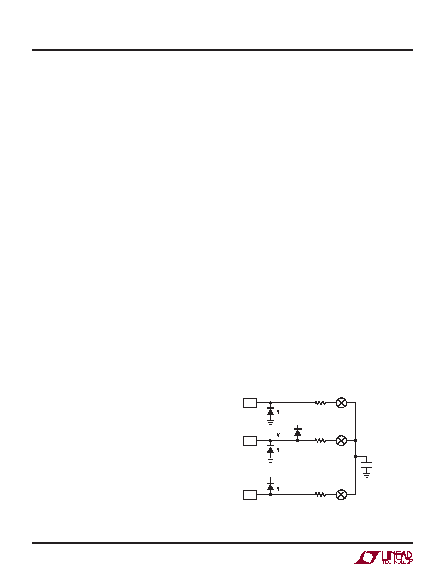
Driving VCC and GND
The VCC and GND pins of the LTC2450 converter are
directly connected to the positive and negative reference
voltages, respectively. A simplied equivalent circuit is
shown in Figure 14.
The power supply current passing through the parasitic
layout resistance associated with these common pins will
modify the ADC reference voltage and thus negatively affect
the converter accuracy. It is thus important to keep the
VCC and GND lines quiet, and to connect these supplies
through very low impedance traces.
In relation to the VCC and GND pins, the LTC2450 com-
bines internal high frequency decoupling with damping
Figure 14. LTC2450 Analog Pins Equivalent Circuit
VCC
ILEAK
RSW (TYP)
15k
CEQ (TYP)
0.35pF
INTERNAL SWITCHING FREQUENCY = 4 MHz
RSW (TYP)
15k
RSW (TYP)
15k
VIN
ILEAK
GND
ILEAK
VCC
2450 F14
相关PDF资料 |
PDF描述 |
|---|---|
| ECM25DCCH | CONN EDGECARD 50POS R/A .156 SLD |
| EBM28DRTI | CONN EDGECARD 56POS DIP .156 SLD |
| ECM25DCCD | CONN EDGECARD 50POS R/A .156 SLD |
| ECM25DCBN | CONN EDGECARD 50POS R/A .156 SLD |
| MLF1608C220M | INDUCTOR MULTILAYER 22UH 0603 |
相关代理商/技术参数 |
参数描述 |
|---|---|
| DC106R | 制造商:未知厂家 制造商全称:未知厂家 功能描述:Analog IC |
| DC107 | 制造商:未知厂家 制造商全称:未知厂家 功能描述:Analog IC |
| DC1073A | 制造商:Linear Technology 功能描述:LT3845EFE DEMO BOARD |
| DC1074A | 功能描述:BOARD DAC LTC2630-12 RoHS:是 类别:编程器,开发系统 >> 评估板 - 数模转换器 (DAC) 系列:QuikEval™ 产品培训模块:Lead (SnPb) Finish for COTS Obsolescence Mitigation Program 标准包装:1 系列:- DAC 的数量:4 位数:12 采样率(每秒):- 数据接口:串行,SPI? 设置时间:3µs DAC 型:电流/电压 工作温度:-40°C ~ 85°C 已供物品:板 已用 IC / 零件:MAX5581 |
| DC1075A | 功能描述:BOARD COMPANION RoHS:是 类别:编程器,开发系统 >> 评估演示板和套件 系列:- 标准包装:1 系列:- 主要目的:数字电位器 嵌入式:- 已用 IC / 零件:AD5258 主要属性:- 次要属性:- 已供物品:板 相关产品:AD5258BRMZ1-ND - IC POT DGTL I2C1K 64P 10MSOPAD5258BRMZ10-ND - IC POT DGTL I2C 10K 64P 10MSOPAD5258BRMZ100-ND - IC POT DGTL I2C 100K 64P 10MSOPAD5258BRMZ50-ND - IC POT DGTL I2C 50K 64P 10MSOPAD5258BRMZ1-R7-ND - IC POT DGTL I2C 1K 64P 10MSOPAD5258BRMZ10-R7-ND - IC POT DGTL I2C 10K 64P 10MSOPAD5258BRMZ50-R7-ND - IC POT DGTL I2C 50K 64P 10MSOPAD5258BRMZ100-R7-ND - IC POT DGTL I2C 100K 64P 10MSOP |
发布紧急采购,3分钟左右您将得到回复。