- 您现在的位置:买卖IC网 > PDF目录20399 > DC1367A (Linear Technology)BOARD EVAL LTM4615 PDF资料下载
参数资料
| 型号: | DC1367A |
| 厂商: | Linear Technology |
| 文件页数: | 15/24页 |
| 文件大小: | 0K |
| 描述: | BOARD EVAL LTM4615 |
| 软件下载: | LTM4615 |
| 设计资源: | DC1367A Design Files DC1367A Schematic |
| 标准包装: | 1 |
| 系列: | LTM®, uModule® |
| 主要目的: | DC/DC,LDO 步降 |
| 输出及类型: | 3,非隔离 |
| 输出电压: | 1.8V,1.2V,1V |
| 电流 - 输出: | 4A,2.5A,1.5A |
| 输入电压: | 2.5 ~ 5.5 V |
| 稳压器拓扑结构: | 降压 |
| 频率 - 开关: | 1.25MHz |
| 板类型: | 完全填充 |
| 已供物品: | 板 |
| 已用 IC / 零件: | LTM4615 |
| 相关产品: | LTM4615EV#PBF-ND - IC SWIT REG BUCK 4A ADJ 144LGA LTM4615IV#PBF-ND - IC SWIT REG BUCK 4A ADJ 144LGA |
�� �
�
�LTM4615�
�APPLICATIONS� INFORMATION�
�Reverse� input� current� will� spike� up� as� LDO_IN� gets� to�
�within� about� 30mV� of� LDO_OUT� as� reverse� current� protec-�
�tion� circuitry� is� disabled� and� normal� operation� resumes.�
�As� LDO_IN� transitions� above� LDO_OUT� the� reverse� current�
�transitions� into� short� circuit� current� as� long� as� LDO_OUT�
�is� held� below� the� regulation� voltage.�
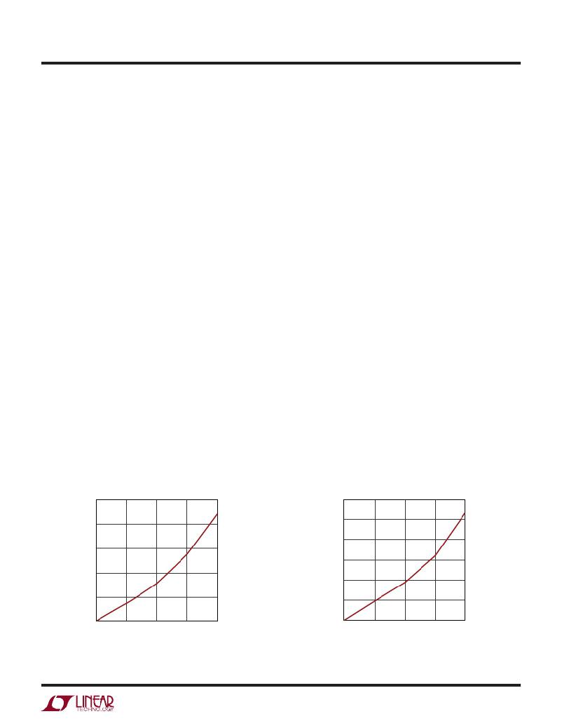
�Thermal� Considerations� and� Output� Current� Derating�
�The� power� loss� curves� in� Figures� 5� and� 6� can� be� used�
�in� coordination� with� the� load� current� derating� curves� in�
�Figures� 7� to� 10� for� calculating� an� approximate� θ� JA� thermal�
�resistance� for� the� LTM4615� with� various� heat� sinking� and�
�airflow� conditions.� Both� of� the� LTM4615� outputs� are� at� full�
�4A� load� current,� and� the� power� loss� curves� in� Figures� 5�
�and� 6� are� combined� power� losses� plotted� for� both� output�
�voltages� up� to� 4A� each.� The� VLDO� regulator� is� set� to� have�
�a� power� dissipation� of� 0.5W� since� it� is� generally� used� with�
�dropout� voltages� of� 0.5V� or� less.� For� example:� 1.2V� to� 1V,�
�1.5V� to� 1V,� 1.5V� to� 1.2V� and� 1.8V� to� 1.5V.� Other� dropout�
�voltages� can� be� supported� at� VLDO� maximum� load,� but�
�further� thermal� analysis� will� be� required� for� the� VLDO.�
�The� 4A� output� voltages� are� 1.2V� and� 3.3V.� These� voltages�
�are� chosen� to� include� the� lower� and� higher� output� voltage�
�ranges� for� correlating� the� thermal� resistance.� Thermal�
�models� are� derived� from� several� temperature� measure-�
�ments� in� a� controlled� temperature� chamber� along� with�
�thermal� modeling� analysis.� The� junction� temperatures� are�
�monitored� while� ambient� temperature� is� increased� with� and�
�without� airflow.� The� junctions� are� maintained� at� ~120°C�
�while� lowering� output� current� or� power� with� increasing�
�ambient� temperature.� The� 120°C� value� is� chosen� to� allow�
�for� a� 5°C� margin� window� relative� to� the� maximum� 125°C�
�limit.� The� decreased� output� current� will� decrease� the� inter-�
�nal� module� loss� as� ambient� temperature� is� increased.� The�
�power� loss� curves� in� Figures� 5� and� 6� show� this� amount� of�
�power� loss� as� a� function� of� load� current� that� is� specified�
�for� both� channels.� The� monitored� junction� temperature� of�
�120°C� minus� the� ambient� operating� temperature� specifies�
�how� much� module� temperature� rise� can� be� allowed.� As�
�an� example,� in� Figure� 7� the� load� current� is� derated� to� 3A�
�for� each� channel� with� 0LFM� at� ~90°C� and� the� power� loss�
�for� both� channels� at� 5V� to� 1.2V� at� 3A� output� is� ~1.4W.�
�Add� the� VDLO� power� loss� of� 0.5W� to� equal� 1.9W.� If� the�
�90°C� ambient� temperature� is� subtracted� from� the� 120°C�
�maximum� junction� temperature,� then� the� difference� of� 30°C�
�divided� by� 1.9W� equals� a� 15.7°C/W� thermal� resistance.�
�Table� 2� specifies� a� 15°C/W� value� which� is� very� close.� Table�
�2� and� Table� 3� provide� equivalent� thermal� resistances� for�
�1.2V� and� 3.3V� outputs� with� and� without� air� flow� and� heat�
�sinking.� The� combined� power� loss� for� the� two� 4A� outputs�
�plus� the� VLDO� power� loss� can� be� summed� together� and�
�multiplied� by� the� thermal� resistance� values� in� Tables� 2� and�
�3� for� module� temperature� rise� under� the� specified� condi-�
�tions.� The� printed� circuit� board� is� a� 1.6mm� thick� four� layer�
�board� with� two� ounce� copper� for� the� two� outer� layers� and� 1�
�ounce� copper� for� the� two� inner� layers.� The� PCB� dimensions�
�are� 95mm� � 76mm.� The� BGA� heat� sinks� are� listed� below�
�Table� 3.� The� data� sheet� lists� the� θ� JC� (Junction� to� Case)�
�thermal� resistances� under� the� Pin� Configuration� diagram.�
�2.5�
�2.0�
�V� IN� = 5V�
�3.0�
�2.5�
�V� IN� = 5V�
�2.0�
�1.5�
�1.5�
�1.0�
�0.5�
�1.0�
�0.5�
�0�
�0�
�1�
�2�
�3�
�4�
�0�
�0�
�1�
�2� 3�
�4�
�15�
�LOAD� CURRENT� (A)�
�4615� F05�
�Figure� 5.� 1.2V� Power� Loss�
�For� more� information� www.linear.com/LTM4615�
�LOAD� CURRENT� (A)�
�4615� F06�
�Figure� 6.� 3.3V� Power� Loss�
�4615fb�
�相关PDF资料 |
PDF描述 |
|---|---|
| R0.25D12-1224/HP-R | CONV DC/DC 0.25W 12VIN +/-24VOUT |
| T95Z226M016LSAL | CAP TANT 22UF 16V 20% 2910 |
| OVP-12G | OVP MOD CASES B,C,N,D,ECT+DATA |
| 412-59584-G | COVER FOR MAP55 & MAP40-1005 |
| R0.25D12-1215/HP-R | CONV DC/DC 0.25W 12VIN +/-15VOUT |
相关代理商/技术参数 |
参数描述 |
|---|---|
| DC1369A-A | 功能描述:BOARD DEMO 125MSPS LTC2261-14 RoHS:是 类别:未定义的类别 >> 其它 系列:* 标准包装:1 系列:* 其它名称:MS305720A |
| DC1369A-B | 功能描述:BOARD DEMO 105MSPS LTC2260-14 RoHS:是 类别:未定义的类别 >> 其它 系列:* 标准包装:1 系列:* 其它名称:MS305720A |
| DC1369A-C | 功能描述:BOARD DEMO 80MSPS LTC2259-14 RoHS:是 类别:未定义的类别 >> 其它 系列:* 标准包装:1 系列:* 其它名称:MS305720A |
| DC1369A-D | 制造商:Linear Technology 功能描述:14BIT ADC Eval Brd, Rq. DC1371 & DC1075 制造商:Linear Technology 功能描述:14BIT ADC Eval Brd, Rq. DC1371 & DC1075; Silicon Manufacturer:Linear Technology; Silicon Core Number:LTC2258-14; Kit Application Type:Data Converter; Application Sub Type:ADC; Kit Contents:Board, Guide |
| DC1369A-E | 制造商:Linear Technology 功能描述:14BIT ADC Eval Brd, Rq. DC1371 & DC1075 制造商:Linear Technology 功能描述:14BIT ADC Eval Brd, Rq. DC1371 & DC1075; Silicon Manufacturer:Linear Technology; Silicon Core Number:LTC2257-14; Kit Application Type:Data Converter; Application Sub Type:ADC; Kit Contents:Board, Guide |
发布紧急采购,3分钟左右您将得到回复。