- 您现在的位置:买卖IC网 > PDF目录17066 > DC745A (Linear Technology)BOARD DELTA SIGMA ADC LTC2433-1 PDF资料下载
参数资料
| 型号: | DC745A |
| 厂商: | Linear Technology |
| 文件页数: | 15/28页 |
| 文件大小: | 0K |
| 描述: | BOARD DELTA SIGMA ADC LTC2433-1 |
| 软件下载: | QuikEval System |
| 设计资源: | DC745A Design File DC745A Schematic |
| 标准包装: | 1 |
| 系列: | QuikEval™ |
| ADC 的数量: | 2 |
| 位数: | 16 |
| 采样率(每秒): | 6.8 |
| 数据接口: | MICROWIRE?,串行,SPI? |
| 工作温度: | 0°C ~ 70°C |
| 已用 IC / 零件: | LTC2433-1 |
| 已供物品: | 板 |
| 相关产品: | LTC2433-1IMS#PBF-ND - IC ADC DIFF 16BIT 3WIRE 10-MSOP LTC2433-1CMS#TRPBF-ND - IC ADC DIFF 16BIT 3WIRE 10-MSOP LTC2433-1IMS#TRPBF-ND - IC ADC DIFF 16BIT 3WIRE 10-MSOP LTC2433-1CMS#PBF-ND - IC ADC DIFF 16BIT 3WIRE 10-MSOP LTC2433-1IMS#TR-ND - IC CONV A/D 16BIT DIFF 10-MSOP LTC2433-1CMS#TR-ND - IC CONV A/D 16BIT DIFF 10-MSOP LTC2433-1IMS-ND - IC CONV A/D 16BIT DIFF 10-MSOP LTC2433-1CMS-ND - IC ADC DIFF 16BIT 3WIRE 10-MSOP |
第1页第2页第3页第4页第5页第6页第7页第8页第9页第10页第11页第12页第13页第14页当前第15页第16页第17页第18页第19页第20页第21页第22页第23页第24页第25页第26页第27页第28页
LTC2433-1
22
24331fa
In addition to this gain error, an offset error term may also
appear. The offset error is proportional with the mismatch
between the source impedance driving the two input pins
IN+ and IN– and with the difference between the input and
reference common mode voltages. While the input drive
circuit nonzero source impedance combined with the con-
verter average input current will not degrade the INL
performance, indirect distortion may result from the modu-
lation of the offset error by the common mode component
of the input signal. Thus, when using large CIN capacitor
values, it is advisable to carefully match the source imped-
ance seen by the IN+ and IN– pins. When FO = LOW
(internal oscillator and 50Hz/60Hz notch), every 180
mismatch in source impedance transforms a full-scale
common mode input signal into a differential mode input
signal of 1LSB. When FO is driven by an external oscillator
with a frequency fEOSC, every 1 mismatch in source
impedance transforms a full-scale common mode input
signal into a differential mode input signal of 3.7 10–8
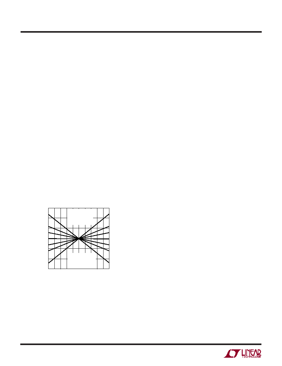
fEOSCLSB. Figure 18 shows the typical offset error due to
input common mode voltage for various values of source
resistance imbalance between the IN+ and IN– pins when
large CIN values are used.
If possible, it is desirable to operate with the input signal
common mode voltage very close to the reference signal
common mode voltage as is the case in the ratiometric
measurement of a symmetric bridge. This configuration
eliminates the offset error caused by mismatched source
impedances.
The magnitude of the dynamic input current depends upon
the size of the very stable internal sampling capacitors and
upon the accuracy of the converter sampling clock. The
accuracy of the internal clock over the entire temperature
and power supply range is typically better than 0.5%. Such
a specification can also be easily achieved by an external
clock. When relatively stable resistors (50ppm/
°C) are
used for the external source impedance seen by IN+ and
IN–, the expected drift of the dynamic current, offset and
gain errors will be insignificant (about 1% of their respec-
tive values over the entire temperature and voltage range).
Even for the most stringent applications, a one-time
calibration operation may be sufficient.
In addition to the input sampling charge, the input ESD
protection diodes have a temperature dependent leakage
current. This current, nominally 1nA (
±10nA max), results
in a small offset shift. A 15k source resistance will create
a 0LSB typical and 1LSB maximum offset voltage.
Reference Current
In a similar fashion, the LTC2433-1 samples the differen-
tial reference pins REF+ and REF– transfering small amount
of charge to and from the external driving circuits thus
producing a dynamic reference current. This current does
not change the converter offset, but it may degrade the
gain and INL performance. The effect of this current can be
analyzed in the same two distinct situations.
For relatively small values of the external reference capaci-
tors (CREF < 0.01F), the voltage on the sampling capacitor
settles almost completely and relatively large values for
the source impedance result in only small errors. Such
values for CREF will deteriorate the converter offset and
gain performance without significant benefits of reference
filtering and the user is advised to avoid them.
Figure 18. Offset Error vs Common Mode Voltage
(VINCM = IN+ = IN–) and Input Source Resistance
Imbalance (
RIN = RSOURCEIN+ – RSOURCEIN–) for
Large CIN Values (CIN ≥ 1F)
VINCM (V)
0
OFFSET
ERROR
(LSB)
3
2
1
0
–1
–2
–3
4
24331 F18
1
C
D
F
0.5
2
1.5
3
3.5
4.5
2.5
5
FO = GND
TA = 25°C
RSOURCEIN– = 500
CIN = 10F
VCC = 5V
REF+ = 5V
REF – = GND
IN+ = IN– = VINCM
A:
RIN = +400
B:
RIN = +200
C:
RIN = +100
D:
RIN = 0
E:
RIN = –100
F:
RIN = –200
G:
RIN = –400
E
B
A
G
APPLICATIO S I FOR ATIO
WU
UU
相关PDF资料 |
PDF描述 |
|---|---|
| RMM08DRXS | CONN EDGECARD 16POS DIP .156 SLD |
| SC75B-100 | INDUCTOR SMD 10UH 2.30A 2.52MHZ |
| RBM11DRAH | CONN EDGECARD 22POS R/A .156 SLD |
| CI160808-12NJ | INDUCTOR 12NH 300MA SMD |
| 0210490986 | CABLE JUMPER 1.25MM .030M 29POS |
相关代理商/技术参数 |
参数描述 |
|---|---|
| DC746A | 功能描述:BOARD DELTA SIGMA ADC LTC2412 RoHS:是 类别:编程器,开发系统 >> 评估板 - 模数转换器 (ADC) 系列:QuikEval™ 产品培训模块:Obsolescence Mitigation Program 标准包装:1 系列:- ADC 的数量:1 位数:12 采样率(每秒):94.4k 数据接口:USB 输入范围:±VREF/2 在以下条件下的电源(标准):- 工作温度:-40°C ~ 85°C 已用 IC / 零件:MAX11645 已供物品:板,软件 |
| DC74HC259 | 制造商:TI 制造商全称:Texas Instruments 功能描述:High Speed CMOS Logic 8-Bit Addressable Latch |
| DC-750 | 制造商:Bivar 功能描述:CARD GUIDE DEEP 7.5" 0.08" BK |
| DC-750-102 | 制造商:Bivar 功能描述:CARD GUIDE DEEP 7.5" 0.102" BK |
| DC-750-102-CI | 制造商:Bivar 功能描述:CARD GUIDE INSERT 7.5" 0.102" BK |
发布紧急采购,3分钟左右您将得到回复。