- 您现在的位置:买卖IC网 > PDF目录17066 > DC745A (Linear Technology)BOARD DELTA SIGMA ADC LTC2433-1 PDF资料下载
参数资料
| 型号: | DC745A |
| 厂商: | Linear Technology |
| 文件页数: | 5/28页 |
| 文件大小: | 0K |
| 描述: | BOARD DELTA SIGMA ADC LTC2433-1 |
| 软件下载: | QuikEval System |
| 设计资源: | DC745A Design File DC745A Schematic |
| 标准包装: | 1 |
| 系列: | QuikEval™ |
| ADC 的数量: | 2 |
| 位数: | 16 |
| 采样率(每秒): | 6.8 |
| 数据接口: | MICROWIRE?,串行,SPI? |
| 工作温度: | 0°C ~ 70°C |
| 已用 IC / 零件: | LTC2433-1 |
| 已供物品: | 板 |
| 相关产品: | LTC2433-1IMS#PBF-ND - IC ADC DIFF 16BIT 3WIRE 10-MSOP LTC2433-1CMS#TRPBF-ND - IC ADC DIFF 16BIT 3WIRE 10-MSOP LTC2433-1IMS#TRPBF-ND - IC ADC DIFF 16BIT 3WIRE 10-MSOP LTC2433-1CMS#PBF-ND - IC ADC DIFF 16BIT 3WIRE 10-MSOP LTC2433-1IMS#TR-ND - IC CONV A/D 16BIT DIFF 10-MSOP LTC2433-1CMS#TR-ND - IC CONV A/D 16BIT DIFF 10-MSOP LTC2433-1IMS-ND - IC CONV A/D 16BIT DIFF 10-MSOP LTC2433-1CMS-ND - IC ADC DIFF 16BIT 3WIRE 10-MSOP |
第1页第2页第3页第4页当前第5页第6页第7页第8页第9页第10页第11页第12页第13页第14页第15页第16页第17页第18页第19页第20页第21页第22页第23页第24页第25页第26页第27页第28页
LTC2433-1
13
24331fa
In addition, the CS signal can be used to trigger a new
conversion cycle before the entire serial data transfer has
been completed. The LTC2433-1 will abort any serial data
transfer in progress and start a new conversion cycle
anytime a LOW-to-HIGH transition is detected at the CS
pin after the converter has entered the data output state
(i.e., after the first rising edge of SCK occurs with
CS = LOW).
Finally, CS can be used to control the free-running modes
of operation, see Serial Interface Timing Modes section.
Grounding CS will force the ADC to continuously convert
at the maximum output rate selected by FO.
SERIAL INTERFACE TIMING MODES
The LTC2433-1’s 3-wire interface is SPI and MICROWIRE
compatible. This interface offers several flexible modes of
operation. These include internal/external serial clock,
2- or 3-wire I/O, single cycle conversion and autostart. The
following sections describe each of these serial interface
timing modes in detail. In all these cases, the converter
can use the internal oscillator (FO = LOW) or an external
oscillator connected to the FO pin. Refer to Table 4 for a
summary.
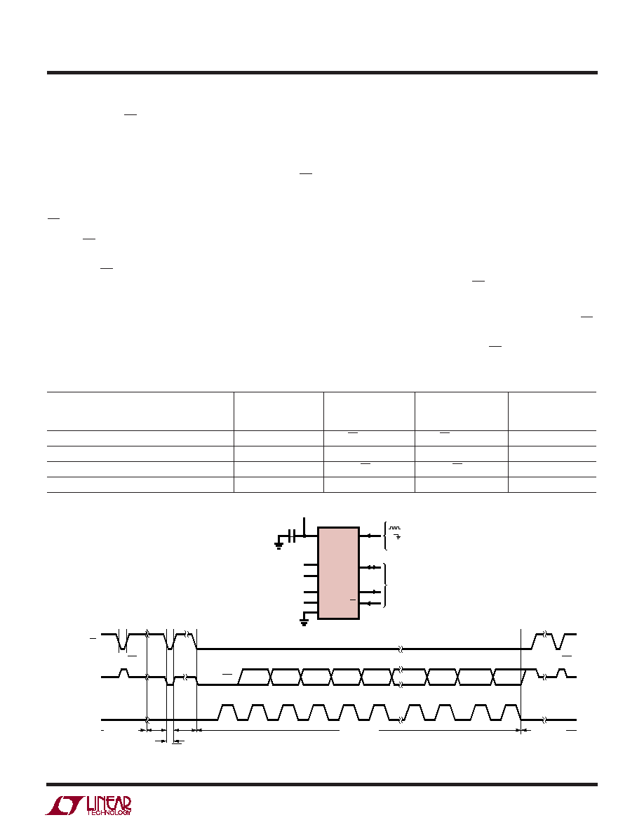
External Serial Clock, Single Cycle Operation
(SPI/MICROWIRE Compatible)
This timing mode uses an external serial clock to shift out
the conversion result and a CS signal to monitor and
control the state of the conversion cycle, see Figure 6.
The serial clock mode is selected on the falling edge of CS.
To select the external serial clock mode, the serial clock pin
(SCK) must be LOW during each CS falling edge.
Figure 6. External Serial Clock, Single Cycle Operation
Table 4. LTC2433-1 Interface Timing Modes
Conversion
Data
Connection
SCK
Cycle
Output
and
Configuration
Source
Control
Waveforms
External SCK, Single Cycle Conversion
External
CS and SCK
Figures 6, 7
External SCK, 2-Wire I/O
External
SCK
Figure 8
Internal SCK, Single Cycle Conversion
Internal
CS
↓
CS
↓
Figures 9, 10
Internal SCK, 2-Wire I/O, Continuous Conversion
Internal
Continuous
Internal
Figure 11
EOC
BIT 18
SDO
SCK
(EXTERNAL)
CS
TEST EOC
MSB
SIG
“O”
BIT 0
LSB
BIT 2
BIT 1
BIT 14
BIT 13
BIT 15
BIT 16
BIT 17
SLEEP
TEST EOC
(OPTIONAL)
DATA OUTPUT
CONVERSION
24331 F06
CONVERSION
Hi-Z
TEST EOC
= EXTERNAL CLOCK SOURCE
= INTERNAL OSC/SIMULTANEOUS
50Hz/60Hz REJECTION
VCC
FO
REF+
REF–
SCK
IN+
IN–
SDO
GND
CS
110
2
3
9
4
5
8
6
7
REFERENCE
VOLTAGE
0.1V TO VCC
ANALOG INPUT RANGE
–0.5VREF TO 0.5VREF
1
F
2.7V TO 5.5V
LTC2433-1
3-WIRE
SPI INTERFACE
APPLICATIO S I FOR ATIO
WU
UU
相关PDF资料 |
PDF描述 |
|---|---|
| RMM08DRXS | CONN EDGECARD 16POS DIP .156 SLD |
| SC75B-100 | INDUCTOR SMD 10UH 2.30A 2.52MHZ |
| RBM11DRAH | CONN EDGECARD 22POS R/A .156 SLD |
| CI160808-12NJ | INDUCTOR 12NH 300MA SMD |
| 0210490986 | CABLE JUMPER 1.25MM .030M 29POS |
相关代理商/技术参数 |
参数描述 |
|---|---|
| DC746A | 功能描述:BOARD DELTA SIGMA ADC LTC2412 RoHS:是 类别:编程器,开发系统 >> 评估板 - 模数转换器 (ADC) 系列:QuikEval™ 产品培训模块:Obsolescence Mitigation Program 标准包装:1 系列:- ADC 的数量:1 位数:12 采样率(每秒):94.4k 数据接口:USB 输入范围:±VREF/2 在以下条件下的电源(标准):- 工作温度:-40°C ~ 85°C 已用 IC / 零件:MAX11645 已供物品:板,软件 |
| DC74HC259 | 制造商:TI 制造商全称:Texas Instruments 功能描述:High Speed CMOS Logic 8-Bit Addressable Latch |
| DC-750 | 制造商:Bivar 功能描述:CARD GUIDE DEEP 7.5" 0.08" BK |
| DC-750-102 | 制造商:Bivar 功能描述:CARD GUIDE DEEP 7.5" 0.102" BK |
| DC-750-102-CI | 制造商:Bivar 功能描述:CARD GUIDE INSERT 7.5" 0.102" BK |
发布紧急采购,3分钟左右您将得到回复。