- 您现在的位置:买卖IC网 > PDF目录17061 > DC846A (Linear Technology)BOARD DELTA SIGMA ADC LTC2447 PDF资料下载
参数资料
| 型号: | DC846A |
| 厂商: | Linear Technology |
| 文件页数: | 24/28页 |
| 文件大小: | 0K |
| 描述: | BOARD DELTA SIGMA ADC LTC2447 |
| 软件下载: | QuikEval System |
| 设计资源: | DC846A Design File DC846A Schematic |
| 标准包装: | 1 |
| 系列: | QuikEval™ |
| ADC 的数量: | 1 |
| 位数: | 24 |
| 采样率(每秒): | 8k |
| 数据接口: | MICROWIRE?,串行,SPI? |
| 已用 IC / 零件: | LTC2447 |
| 已供物品: | 板 |
| 相关产品: | LTC2447IUHF#PBF-ND - IC ADC 24BIT 8CH HI SPEED 38QFN LTC2447CUHF#PBF-ND - IC ADC 24BIT 8CH HI SPEED 38QFN LTC2447IUHF#TRPBF-ND - IC ADC 24BIT 8CH HI SPEED 38QFN LTC2447CUHF#TRPBF-ND - IC ADC 24BIT 8CH HI SPEED 38QFN |
第1页第2页第3页第4页第5页第6页第7页第8页第9页第10页第11页第12页第13页第14页第15页第16页第17页第18页第19页第20页第21页第22页第23页当前第24页第25页第26页第27页第28页
LTC2446/LTC2447
5
24467fa
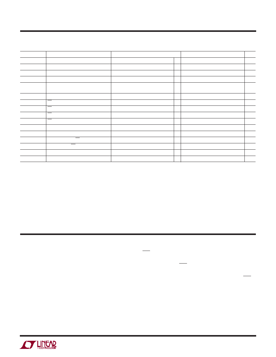
SYMBOL
PARAMETER
CONDITIONS
MIN
TYP
MAX
UNITS
DISCK
Internal SCK Duty Cycle
(Note 9)
●
45
55
%
fESCK
External SCK Frequency Range
(Note 8)
●
20
MHz
tLESCK
External SCK Low Period
(Note 8)
●
25
ns
tHESCK
External SCK High Period
(Note 8)
●
25
ns
tDOUT_ISCK
Internal SCK 32-Bit Data Output Time
Internal Oscillator (Notes 9, 11)
●
41.6
35.3
30.9
s
External Oscillator (Notes 9, 10)
●
320/fEOSC
s
tDOUT_ESCK
External SCK 32-Bit Data Output Time
(Note 8)
●
32/fESCK
s
t1
CS
↓ to SDO Low Z
(Note 12)
●
025
ns
t2
CS
↑ to SDO High Z
(Note 12)
●
025
ns
t3
CS
↓ to SCK ↓
(Note 9)
5
s
t4
CS
↓ to SCK ↑
(Notes 8, 12)
●
25
ns
tKQMAX
SCK
↓ to SDO Valid
●
25
ns
tKQMIN
SDO Hold After SCK
↓
(Note 5)
●
15
ns
t5
SCK Setup Before CS
↓
●
50
ns
t6
SCK Hold After CS
↓
●
50
ns
t7
SDI Setup Before SCK
↑
(Note 5)
●
10
ns
t8
SDI Hold After SCK
↑
(Note 5)
●
10
ns
The
● denotes specifications which apply over the full operating temperature
range, otherwise specifications are at TA = 25°C. (Note 3)
TI I G CHARACTERISTICS
W
U
GND (Pins 1, 4, 5, 6, 31, 32, 33): Ground. Multiple
ground pins internally connected for optimum ground
current flow and VCC decoupling. Connect each one of
these pins to a common ground plane through a low
impedance connection. All seven pins must be connected
to ground for proper operation.
BUSY (Pin 2): Conversion in Progress Indicator. This pin
is HIGH while the conversion is in progress and goes LOW
indicating the conversion is complete and data is ready. It
remains LOW during the sleep and data output states. At
the conclusion of the data output state, it goes HIGH
indicating a new conversion has begun.
EXT (Pin 3): Internal/External SCK Selection Pin. This pin
is used to select internal or external SCK for outputting/
inputting data. If EXT is tied low, the device is in the
external SCK mode and data is shifted out of the device
under the control of a user applied serial clock. If EXT is
tied high, the internal serial clock mode is selected. The
device generates its own SCK signal and outputs this on
the SCK pin. A framing signal BUSY (Pin 2) goes low
indicating data is being output.
COM (Pin 7): The common negative input (IN–) for all
single ended multiplexer configurations. The voltage on
CH0-CH7 and COM pins can have any value between GND
UU
U
PI FU CTIO S
Note 1: Absolute Maximum Ratings are those values beyond which the life
of the device may be impaired.
Note 2: All voltage values are with respect to GND.
Note 3: VCC = 4.5V to 5.5V unless otherwise specified.
VREF = REF+ – REF–, VREFCM = (REF+ + REF–)/2; REF+ is the positive
reference input, REF– is the negative reference input; VIN = IN
+ – IN–,
VINCM = (IN+ + IN–)/2.
Note 4: FO pin tied to GND or to external conversion clock source with
fEOSC = 10MHz unless otherwise specified.
Note 5: Guaranteed by design, not subject to test.
Note 6: Integral nonlinearity is defined as the deviation of a code from a
straight line passing through the actual endpoints of the transfer curve.
The deviation is measured from the center of the quantization band.
Note 7: The converter uses the internal oscillator.
Note 8: The converter is in external SCK mode of operation such that the
SCK pin is used as a digital input. The frequency of the clock signal driving
SCK during the data output is fESCK and is expressed in Hz.
Note 9: The converter is in internal SCK mode of operation such that the
SCK pin is used as a digital output. In this mode of operation, the SCK pin
has a total equivalent load capacitance of CLOAD = 20pF.
Note 10: The external oscillator is connected to the FO pin. The external
oscillator frequency, fEOSC, is expressed in Hz.
Note 11: The converter uses the internal oscillator. FO = 0V.
Note 12: Guaranteed by design and test correlation.
Note 13: There is an internal reset that adds an additional 1
s (typ) to the
conversion time.
相关PDF资料 |
PDF描述 |
|---|---|
| LGN2H680MELZ30 | CAP ALUM 68UF 500V 20% SNAP |
| VE-B20-EY | CONVERTER MOD DC/DC 5V 50W |
| DC956A | BOARD DELTA SIGMA ADC LTC2485 |
| VE-B21-EY | CONVERTER MOD DC/DC 12V 50W |
| DC571A | BOARD DELTA SIGMA ADC LTC2418 |
相关代理商/技术参数 |
参数描述 |
|---|---|
| DC847A | 功能描述:BOARD DELTA SIGMA ADC LTC2446 RoHS:是 类别:编程器,开发系统 >> 评估板 - 模数转换器 (ADC) 系列:QuikEval™ 产品培训模块:Obsolescence Mitigation Program 标准包装:1 系列:- ADC 的数量:1 位数:12 采样率(每秒):94.4k 数据接口:USB 输入范围:±VREF/2 在以下条件下的电源(标准):- 工作温度:-40°C ~ 85°C 已用 IC / 零件:MAX11645 已供物品:板,软件 |
| DC850 | 制造商:Molex 功能描述: |
| DC852A | 功能描述:BOARD DEMO FOR LTC4354 RoHS:是 类别:未定义的类别 >> 其它 系列:* 标准包装:1 系列:* 其它名称:MS305720A |
| DC8550 | 制造商:DCCOM 制造商全称:Dc Components 功能描述:TECHNICAL SPECIFICATIONS OF PNP EPITAXIAL PLANAR TRANSISTOR |
| DC8550S | 制造商:DCCOM 制造商全称:Dc Components 功能描述:TECHNICAL SPECIFICATIONS OF PNP EPITAXIAL PLANAR TRANSISTOR |
发布紧急采购,3分钟左右您将得到回复。