- 您现在的位置:买卖IC网 > PDF目录9265 > DS1023S-50/T&R (Maxim Integrated Products)IC DELAY LINE 256TAP 16-SOIC PDF资料下载
参数资料
| 型号: | DS1023S-50/T&R |
| 厂商: | Maxim Integrated Products |
| 文件页数: | 10/16页 |
| 文件大小: | 0K |
| 描述: | IC DELAY LINE 256TAP 16-SOIC |
| 产品培训模块: | Lead (SnPb) Finish for COTS Obsolescence Mitigation Program |
| 标准包装: | 1,000 |
| 标片/步级数: | 256 |
| 功能: | 单发射,可编程 |
| 延迟到第一抽头: | 16.5ns |
| 接头增量: | 0.5ns |
| 可用的总延迟: | 127.5ns |
| 独立延迟数: | 1 |
| 电源电压: | 4.75 V ~ 5.25 V |
| 工作温度: | 0°C ~ 70°C |
| 安装类型: | 表面贴装 |
| 封装/外壳: | 16-SOIC(0.295",7.50mm 宽) |
| 供应商设备封装: | 16-SOIC W |
| 包装: | 带卷 (TR) |
DS1023
3 of 16
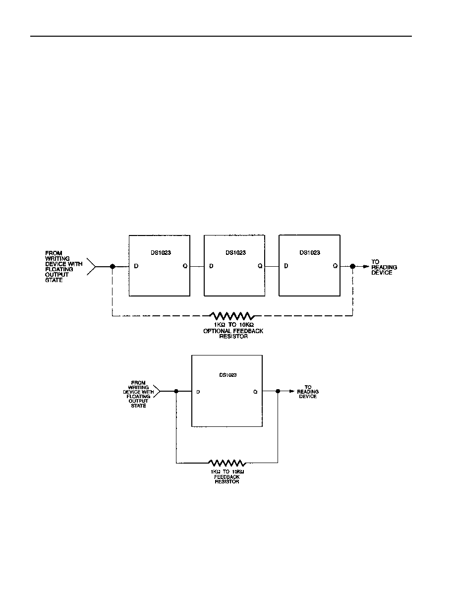
Applications can read the setting of the DS1023 Delay Line by connecting the serial output pin (Q) to the
serial input (D) through a resistor with a value of 1 to 10 kohms (Figure 2). Since the read process is
destructive, the resistor restores the value read and provides isolation when writing to the device. The
resistor must connect the serial output (Q) of the last device to the serial input (D) of the first device of a
daisy chain (Figure 1). For serial readout with automatic restoration through a resistor, the device used to
write serial data must go to a high impedance state.
To initiate a serial read, latch enable (LE) is taken to a logic 1 while serial clock (CLK) is at a logic 0.
After a waiting time (tEQV), bit 7 (MSB) appears on the serial output (Q). On the first rising (0 --> 1)
transition of the serial clock (CLK), bit 7 (MSB) is rewritten and bit 6 appears on the output after a time
tCQV. To restore the input register to its original state, this clocking process must be repeated eight times.
In the case of a daisy chain, the process must be repeated eight times per package. If the value read is
restored before latch enable (LE) is returned to logic 0, no settling time (tEDV) is required and the
programmed delay remains unchanged.
Since the DS1023 is a CMOS design, unused input pins (P3 - P7) must be connected to well-defined logic
levels; they must not be allowed to float. Serial output Q/P0 should be allowed to float if unused.
CASCADING MULTIPLE DEVICES (DAISY CHAIN) Figure 1
SERIAL READOUT Figure 2
REFERENCE DELAY
In all delay lines there is an inherent, or “step zero”, delay caused by the propagation delay through the
input and output buffers. In this device the step zero delay can be quite large compared to the delay step
size. To simplify system design a reference delay has been included on chip which may be used to
compensate for the step zero delay. In practice this means that if the device is supplied with a clock, for
example, the minimum programmed output delay is effectively zero with respect to the reference delay.
相关PDF资料 |
PDF描述 |
|---|---|
| VI-25R-MX-B1 | CONVERTER MOD DC/DC 7.5V 75W |
| DS1023S-200 | IC DELAY LINE 256TAP 16-SOIC |
| VE-B6F-MY-F4 | CONVERTER MOD DC/DC 72V 50W |
| VE-B6F-MY-F2 | CONVERTER MOD DC/DC 72V 50W |
| CAT5172TBI-00GT3 | IC POT DGTL 100K 256TAP SOT23-8 |
相关代理商/技术参数 |
参数描述 |
|---|---|
| DS10-24B | 制造商:TRANSMISSION DEVELOPMENTS 功能描述:MOULDED SPUR GEAR 1.0, 24 |
| DS1027AS | 制造商:Maxim Integrated Products 功能描述:DS1027AS |
| DS102-K | 制造商:Miyama Electric 功能描述: |
| DS102-M | 制造商:Miyama Electric 功能描述: |
| DS102OS-50 | 制造商:Maxim Integrated Products 功能描述: |
发布紧急采购,3分钟左右您将得到回复。