- 您现在的位置:买卖IC网 > PDF目录9172 > DS1856B-M50+ (Maxim Integrated Products)IC DGTL POT 50K 256TAPS 16CSBGA PDF资料下载
参数资料
| 型号: | DS1856B-M50+ |
| 厂商: | Maxim Integrated Products |
| 文件页数: | 5/31页 |
| 文件大小: | 0K |
| 描述: | IC DGTL POT 50K 256TAPS 16CSBGA |
| 产品培训模块: | Obsolescence Mitigation Program |
| 标准包装: | 100 |
| 接片: | 256 |
| 电阻(欧姆): | 50k |
| 电路数: | 2 |
| 温度系数: | 标准值 50 ppm/°C |
| 存储器类型: | 非易失 |
| 接口: | 2 线串口 |
| 电源电压: | 2.85 V ~ 5.5 V |
| 工作温度: | -40°C ~ 95°C |
| 安装类型: | 表面贴装 |
| 封装/外壳: | 16-LBGA,CSPBGA |
| 供应商设备封装: | 16-CSBGA(4x4) |
| 包装: | 托盘 |
第1页第2页第3页第4页当前第5页第6页第7页第8页第9页第10页第11页第12页第13页第14页第15页第16页第17页第18页第19页第20页第21页第22页第23页第24页第25页第26页第27页第28页第29页第30页第31页
Dual, Temperature-Controlled Resistors with Inter-
nally Calibrated Monitors and Password Protection
Maxim Integrated
13
DS1856
The DS1856 2-wire interface uses 8-bit addressing,
which allows up to 256 bytes to be addressed tradi-
tionally on a given 2-wire slave address. However,
since the Main Device contains more than 256 bytes, a
table scheme is used. The lower 128 bytes of the Main
Device, memory locations 00h to 7Fh, function as
expected and are independent of the currently select-
ed table. Byte 7Fh is the Table Select byte. This byte
determines which memory table will be accessed by
the 2-wire interface when address locations 80h to FFh
are accessed. Memory locations 80h to FFh are acces-
sible only through the Main Device address. The
Auxiliary Device address has no access to the tables,
but the Auxiliary Device memory can be mapped into
the Main Device’s memory space (by setting ADEN =
1). Valid values for the Table Select byte are shown in
the table below.
Before attempting to read and write any of the bits or
bytes mentioned in this section, it is important to look at
the memory map provided in a subsequent section to
verify what level of password is required. Password
protection is described in the following section.
Password Protection
The DS1856 uses two 4-byte passwords to achieve
three levels of access to various memory locations. The
three levels of access are:
User Access: This is the default state after power-up. It
allows read access to standard monitoring and status
functions.
Level 1 Access: This allows access to customer data
table (Tables 00 and 01) in addition to everything grant-
ed by User access. This level is granted by entering
Password 1 (PW1).
Level 2 Access: This allows access to all memory, set-
tings, and features, in addition to everything granted by
Level 1 and User access. This level is granted by enter-
ing Password 2 (PW2).
To obtain a particular level of access, the correspond-
ing password must be entered in the Password Entry
(PWE) bytes located in the Main Device at 7Bh to 7Eh.
The value entered is compared to both the PW1 and
PW2 settings located in Table 03, bytes B0h to B3h and
Table 03, bytes B4h to B7h, respectively, to determine
if access should be granted. Access is granted until
the password is changed or until power is cycled.
Writing PWE can be done with any level of access,
although PWE can never be read.
Writing PW1 and PW2 requires PW2 access. However,
PW1 and PW2 can never be read, even with PW2 access.
On power-up, PWE is set to all 1s (FFFFh). As long as
neither of the passwords are ever changed to FFFFh,
then User access is the power-up default. Likewise,
password protection can be intentionally disabled by
setting the PW2 password to FFFFh.
Memory Map
The following table is the legend used in the memory
map to indicate the access level required for read and
write access.
Each table in the following memory map begins with a
higher level view of a particular portion of the memory
showing information such as row (8 bytes) and byte
names. The tables are then followed, where applicable,
by an Expanded Bytes table, which shows bit names
and values. Furthermore, both tables use the permis-
sion legend to indicate the access required on a row,
byte, and bit level.
The memory map is followed by a
Register Description
section, which describes bytes and bits in further detail.
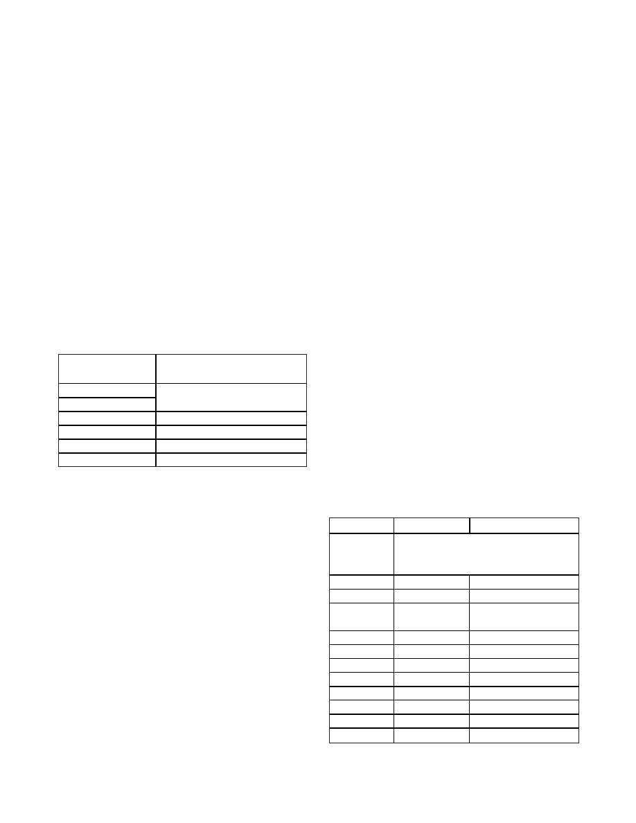
TABLE SELECT
BYTE
TABLE NAME
00
01
Auxiliary Device Memory
(When ADEN = 1)
02
Does Not Exist
03
Configuration
04
Resistor 0 Look-up Table
05
Resistor 1 Look-up Table
PERMISSION
READ
WRITE
<0>
At least one byte in the row is different than
the rest of the row, so look at each byte
separately for permissions.
<1>
all
PW2
<2>
all
NA
<3>
all
all (The part also writes to
this byte.)
<4>
PW2
PW2 + mode_bit
<5>
all
<6>
NA
all
<7>
PW1
<8>
PW2
<9>
NA
PW2
<10>
PW2
NA
<11>
all
PW1
Table 6. Table Select Byte
Table 7. Password Permission
相关PDF资料 |
PDF描述 |
|---|---|
| V72A8H300BL | CONVERTER MOD DC/DC 8V 300W |
| DS1856E-M50+ | IC DGTL POT 50K 256TAPS 16TSSOP |
| MS27466T23B2P | CONN RCPT 85POS WALL MT W/PINS |
| MS3114P18-11S | CONN RCPT 11POS JAM NUT W/SCKT |
| VE-BWP-MY-F1 | CONVERTER MOD DC/DC 13.8V 50W |
相关代理商/技术参数 |
参数描述 |
|---|---|
| DS1856B-M50/T | 制造商:Maxim Integrated Products 功能描述:- Tape and Reel |
| DS1856B-M50/T&R | 制造商:Maxim Integrated Products 功能描述:DUALTEMP 50K,3MON BGA FULL A0/A2M T - Tape and Reel 制造商:Maxim Integrated Products 功能描述:IC DGTL POT 50K 2CH 16CSBGA 制造商:Maxim Integrated Products 功能描述:Digital Potentiometer ICs Extremely Acc SPI Bus RTC |
| DS1856B-M50+ | 功能描述:数字电位计 IC DUALTEMP 50K3MON W/FULL AO/A2 MEMORY RoHS:否 制造商:Maxim Integrated 电阻:200 Ohms 温度系数:35 PPM / C 容差:25 % POT 数量:Dual 每 POT 分接头:256 弧刷存储器:Volatile 缓冲刷: 数字接口:Serial (3-Wire, SPI) 描述/功能:Dual Volatile Low Voltage Linear Taper Digital Potentiometer 工作电源电压:1.7 V to 5.5 V 电源电流:27 uA 最大工作温度:+ 125 C 安装风格:SMD/SMT 封装 / 箱体:TQFN-16 封装:Reel |
| DS1856B-M50+R | 制造商:MAXIM 制造商全称:Maxim Integrated Products 功能描述:Dual, Temperature-Controlled Resistors with Calibrated Monitors and Password Protection |
| DS1856B-M50+T | 制造商:Maxim Integrated Products 功能描述:DUALTEMP 50K,3MON BGA W/FULL AO/A2 MEMORY - Tape and Reel |
发布紧急采购,3分钟左右您将得到回复。