- 您现在的位置:买卖IC网 > PDF目录20026 > DS1863E+ (Maxim Integrated)IC LASR CTRLR 1CHAN 5.5V 16TSSOP PDF资料下载
参数资料
| 型号: | DS1863E+ |
| 厂商: | Maxim Integrated |
| 文件页数: | 17/62页 |
| 文件大小: | 0K |
| 描述: | IC LASR CTRLR 1CHAN 5.5V 16TSSOP |
| 产品培训模块: | Lead (SnPb) Finish for COTS Obsolescence Mitigation Program |
| 标准包装: | 96 |
| 类型: | 激光二极管控制器 |
| 通道数: | 1 |
| 电源电压: | 2.85 V ~ 5.5 V |
| 电流 - 电源: | 5mA |
| 电流 - 偏置: | 1.2mA |
| 工作温度: | -40°C ~ 95°C |
| 封装/外壳: | 16-TSSOP(0.173",4.40mm 宽) |
| 供应商设备封装: | 16-TSSOP |
| 包装: | 管件 |
| 安装类型: | 表面贴装 |
| 产品目录页面: | 1429 (CN2011-ZH PDF) |
第1页第2页第3页第4页第5页第6页第7页第8页第9页第10页第11页第12页第13页第14页第15页第16页当前第17页第18页第19页第20页第21页第22页第23页第24页第25页第26页第27页第28页第29页第30页第31页第32页第33页第34页第35页第36页第37页第38页第39页第40页第41页第42页第43页第44页第45页第46页第47页第48页第49页第50页第51页第52页第53页第54页第55页第56页第57页第58页第59页第60页第61页第62页
�� �
�
�Burst-Mode� PON� Controller�
�With� Integrated� Monitoring�
�specific� memory� address� to� begin� a� data� transfer.� A�
�repeated� START� condition� is� issued� identically� to� a� nor-�
�mal� START� condition.� See� the� timing� diagram� for�
�applicable� timing.�
�Bit� Write:� Transitions� of� SDA� must� occur� during� the� low�
�state� of� SCL.� The� data� on� SDA� must� remain� valid� and�
�unchanged� during� the� entire� high� pulse� of� SCL� plus� the�
�setup� and� hold-time� requirements� (Figure� 9).� Data� is� shift-�
�ed� into� the� device� during� the� rising� edge� of� the� SCL.�
�Bit� Read:� At� the� end� of� a� write� operation,� the� master�
�must� release� the� SDA� bus� line� for� the� proper� amount� of�
�setup� time� before� the� next� rising� edge� of� SCL� during� a�
�bit� read.� The� device� shifts� out� each� bit� of� data� on� SDA� at�
�the� falling� edge� of� the� previous� SCL� pulse� and� the� data�
�bit� is� valid� at� the� rising� edge� of� the� current� SCL� pulse.�
�Remember� that� the� master� generates� all� SCL� clock�
�pulses� including� when� it� is� reading� bits� from� the� slave.�
�Acknowledgement� (ACK� and� NACK):� An� Acknowledge-�
�ment� (ACK)� or� Not� Acknowledge� (NACK)� is� always� the�
�9th� bit� transmitted� during� a� byte� transfer.� The� device�
�receiving� data� (the� master� during� a� read� or� the� slave�
�during� a� write� operation)� performs� an� ACK� by� transmit-�
�ting� a� zero� during� the� 9th� bit.� A� device� performs� a�
�NACK� by� transmitting� a� one� during� the� 9th� bit.� Timing�
�for� the� ACK� and� NACK� is� identical� to� all� other� bit� writes.�
�An� ACK� is� the� acknowledgment� that� the� device� is� prop-�
�erly� receiving� data.� A� NACK� is� used� to� terminate� a� read�
�sequence� or� as� an� indication� that� the� device� is� not�
�receiving� data.�
�Byte� Write:� A� byte� write� consists� of� 8� bits� of� information�
�transferred� from� the� master� to� the� slave� (most� signifi-�
�cant� bit� first)� plus� a� 1-bit� acknowledgement� from� the�
�slave� to� the� master.� The� 8� bits� transmitted� by� the� mas-�
�ter� are� done� according� to� the� bit� write� definition� and� the�
�acknowledgement� is� read� using� the� bit� read� definition.�
�Byte� Read:� A� byte� read� is� an� 8-bit� information� transfer�
�from� the� slave� to� the� master� plus� a� 1-bit� ACK� or� NACK�
�from� the� master� to� the� slave.� The� 8� bits� of� information�
�that� are� transferred� (most� significant� bit� first)� from� the�
�slave� to� the� master� are� read� by� the� master� using� the� bit�
�read� definition,� and� the� master� transmits� an� ACK� using�
�the� bit� write� definition� to� receive� additional� data� bytes.�
�The� master� must� NACK� the� last� byte� read� to� terminate�
�communication� so� the� slave� will� return� control� of� SDA� to�
�the� master.�
�Slave� Address� Byte:� Each� slave� on� the� I� 2� C� bus�
�responds� to� a� slave� addressing� byte� (Figure� 10)� sent�
�immediately� following� a� START� condition.� The� slave�
�address� byte� contains� the� slave� address� in� the� most� sig-�
�nificant� 7� bits� and� the� R/� W� bit� in� the� least� significant� bit.�
�The� DS1863� ’� s� slave� address� can� be� configured� to� any�
�value� between� 00h� to� FEh� using� the� Device� Address�
�Byte� (Table� 02h,� Register� 8Ch).� The� user� also� has� to� set�
�the� ASEL� bit� (Table� 02h,� Register� 89h)� for� this� address� to�
�be� active.� The� default� address� is� A2h� (see� Figure� 10).� By�
�writing� the� correct� slave� address� with� R/� W� =� 0,� the� mas-�
�ter� indicates� it� will� write� data� to� the� slave.� If� R/� W� =� 1,� the�
�master� will� read� data� from� the� slave.� If� an� incorrect� slave�
�address� is� written,� the� DS1863� will� assume� the� master� is�
�communicating� with� another� I� 2� C� device� and� ignore� the�
�communications� until� the� next� START� condition� is� sent.�
�Memory� Address:� During� an� I� 2� C� write� operation,� the�
�master� must� transmit� a� memory� address� to� identify� the�
�memory� location� where� the� slave� is� to� store� the� data.�
�The� memory� address� is� always� the� second� byte� trans-�
�mitted� during� a� write� operation� following� the� slave�
�address� byte.�
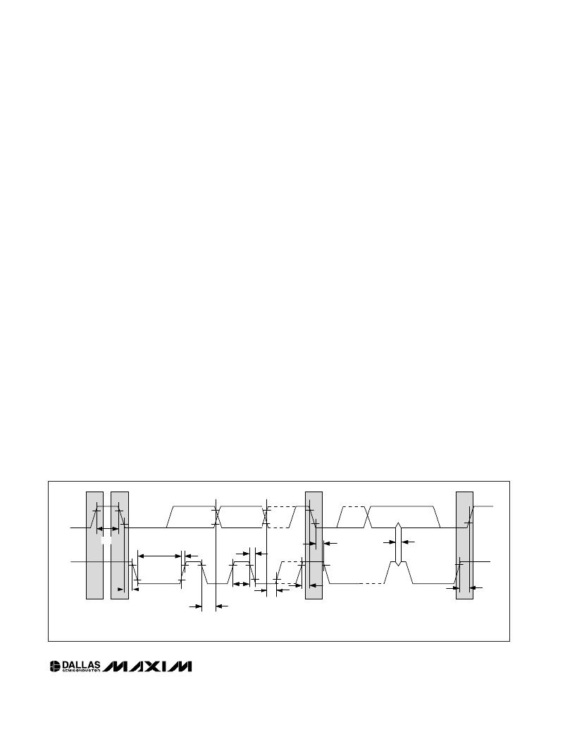
�SDA�
�t� BUF�
�t� HD:STA�
�t� SP�
�SCL�
�t� LOW�
�t� R�
�t� F�
�t� HD:STA�
�t� HIGH�
�t� SU:STA�
�STOP�
�START�
�t� SU:DAT�
�REPEATED�
�START�
�t� SU:STO�
�t� HD:DAT�
�NOTE:� TIMING� IS� REFERENCED� TO� V� IL(MAX)� AND� V� IH(MIN)� .�
�Figure� 9.� I� 2� C� Timing� Diagram.�
�____________________________________________________________________�
�17�
�相关PDF资料 |
PDF描述 |
|---|---|
| TCJP476M006R0500 | CAP TANT 47UF 6.3V 20% 0805 |
| VI-20P-CX | CONVERTER MOD DC/DC 13.8V 75W |
| ECM12DTBH | CONN EDGECARD 24POS R/A .156 SLD |
| 5749111-4 | CONN 50POS .050 CHAMPPLUG SCHCVR |
| TPSD157M010R0050 | CAP TANT 150UF 10V 20% 2917 |
相关代理商/技术参数 |
参数描述 |
|---|---|
| DS1863E+ | 功能描述:激光驱动器 Burst-Mode PON Ctlr w/Integrated Mntr RoHS:否 制造商:Micrel 数据速率:4.25 Gbps 工作电源电压:3 V to 3.6 V 电源电流:80 mA 最大工作温度:+ 85 C 封装 / 箱体:QFN-16 封装:Tube |
| DS1863E+R | 制造商:MAXIM 制造商全称:Maxim Integrated Products 功能描述:Burst-Mode PON Controller With Integrated Monitoring |
| DS1863E+T | 制造商:MAXIM 制造商全称:Maxim Integrated Products 功能描述:Burst-Mode PON Controller With Integrated Monitoring |
| DS1863E+T&R | 制造商:Maxim Integrated Products 功能描述: 制造商:Maxim Integrated Products 功能描述:BURST CNTRLR 16TSSOP - Tape and Reel 制造商:Maxim Integrated Products 功能描述:IC LASR CTRLR 1CHAN 5.5V 16TSSOP |
| DS1863E+T&R | 功能描述:激光驱动器 Burst-Mode PON Ctlr w/Integrated Mntr RoHS:否 制造商:Micrel 数据速率:4.25 Gbps 工作电源电压:3 V to 3.6 V 电源电流:80 mA 最大工作温度:+ 85 C 封装 / 箱体:QFN-16 封装:Tube |
发布紧急采购,3分钟左右您将得到回复。