- 您现在的位置:买卖IC网 > PDF目录20027 > DS1864T+ (Maxim Integrated)IC LASER CTRLR 1CHAN 5.5V 28TQFN PDF资料下载
参数资料
| 型号: | DS1864T+ |
| 厂商: | Maxim Integrated |
| 文件页数: | 19/72页 |
| 文件大小: | 0K |
| 描述: | IC LASER CTRLR 1CHAN 5.5V 28TQFN |
| 产品培训模块: | Lead (SnPb) Finish for COTS Obsolescence Mitigation Program |
| 标准包装: | 60 |
| 类型: | 激光二极管控制器(光纤) |
| 通道数: | 1 |
| 电源电压: | 2.97 V ~ 5.5 V |
| 电流 - 电源: | 3mA |
| 工作温度: | -40°C ~ 95°C |
| 封装/外壳: | 28-WFQFN 裸露焊盘 |
| 供应商设备封装: | 28-TQFN-EP(5x5) |
| 包装: | 管件 |
| 安装类型: | 表面贴装 |
第1页第2页第3页第4页第5页第6页第7页第8页第9页第10页第11页第12页第13页第14页第15页第16页第17页第18页当前第19页第20页第21页第22页第23页第24页第25页第26页第27页第28页第29页第30页第31页第32页第33页第34页第35页第36页第37页第38页第39页第40页第41页第42页第43页第44页第45页第46页第47页第48页第49页第50页第51页第52页第53页第54页第55页第56页第57页第58页第59页第60页第61页第62页第63页第64页第65页第66页第67页第68页第69页第70页第71页第72页
�� �
�
�SFP� Laser� Controller� and�
�Diagnostic� IC�
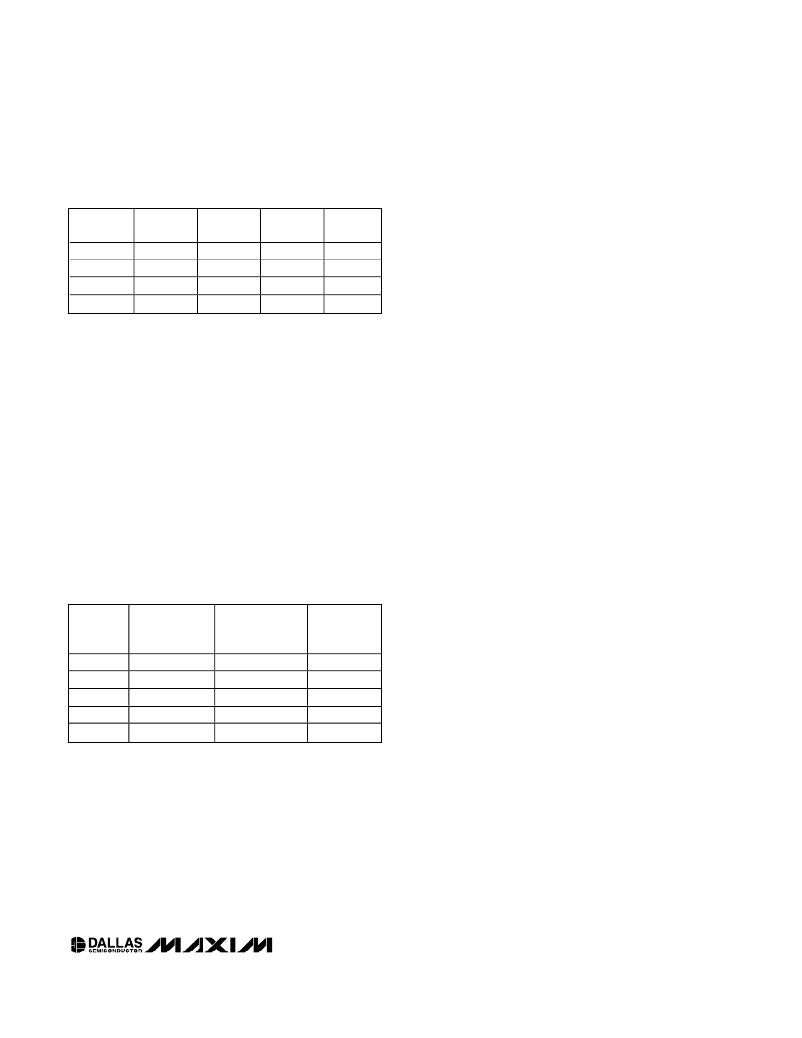
�Table� 4.� Voltage� Monitor� Factory� Default�
�Calibration�
�input� that� would� produce� a� digital� result� of� all� zeros� is�
�the� null� value� (normally� this� input� is� GND).� The� input�
�that� would� produce� a� digital� result� of� all� ones� (FFF8h)� is�
�SIGNAL�
�V� CC�
�MON1�
�MON2�
�MON3�
�+FS�
�(V)�
�6.5528V�
�2.4997V�
�2.4997V�
�2.4997V�
�+FS�
�(hex)�
�FFF8�
�FFF8�
�FFF8�
�FFF8�
�-FS�
�(V)�
�0V�
�0V�
�0V�
�0V�
�-FS�
�(hex)�
�0000�
�0000�
�0000�
�0000�
�the� full-scale� (FS)� value.� The� expected� FS� value� is� also�
�found� by� multiplying� FFF8h� by� the� LSB� weight.�
�The� right-shifting� operation� on� the� A/D� converter� output�
�is� carried� out� based� on� the� contents� of� Registers� Right�
�Shift1� and� Right� Shift2� in� EEPROM.� Each� of� the� three�
�analog� channels� (MON1� (Bias� Current� (IBI)),� MON2�
�(Transmitted� Power� (TXP)),� and� MON3� (Received� Power�
�(RIN))� is� allocated� 3� bits� to� set� the� number� of� right� shifts.�
�To� calculate� the� voltage� measured� from� the� register�
�value,� first� calculate� the� LSB� weight� of� the� 16-bit� register.�
�The� LSB� weight� is� equal� to� the� full-scale� voltage� span�
�divided� 65528.� Next,� convert� the� hexadecimal� register�
�value� to� decimal� and� multiply� it� times� the� LSB� weight.�
�Example:� Using� the� factory� default� V� CC� trim,� what� volt-�
�age� is� measured� if� the� V� CC� register� value� is� C340h?�
�The� LSB� for� V� CC� is� equal� to� (6.5528V� -� 0V)� /� 65528� =�
�100.00μV.� C340h� is� equal� to� 49984� decimal,� which�
�yields� a� supply� voltage� equal� to� 49984� x� 100.00μV� =�
�4.9984V.� Table� 5� shows� more� conversion� examples�
�based� on� the� factory� trimmed� A/D� settings.�
�The� factory-programmed� LSB� for� V� CC� is� 100μV.� The�
�factory-programmed� LSB� weight� for� the� MON� channels�
�is� 38.147μV.�
�Table� 5.� Voltage� Monitor� Conversion�
�Examples�
�Up� to� 7� right-shift� operations� are� allowed� and� will� be�
�executed� as� a� part� of� every� conversion� before� the� result�
�is� loaded� in� the� corresponding� measurement� registers�
�62h� to� 69h.� This� is� true� during� the� setup� of� internal� cali-�
�bration� as� well� as� during� subsequent� data� conversions.�
�Example:� Since� the� FS� digital� reading� is� 65528� (FFF8h)�
�LSBs,� if� the� LSB’s� weight� is� 50μV,� then� the� FS� value� is�
�65528� x� 50μV� =� 3.2764V.�
�A� binary� search� is� used� to� calibrate� the� gain� of� the� con-�
�verter.� This� requires� forcing� two� known� voltages� on� the�
�input� pin.� It� is� preferred� that� one� of� the� forced� voltages� is�
�the� null� input� and� the� other� is� 90%� of� FS.� Since� the� LSB�
�of� the� least� significant� bit� in� the� digital� reading� register� is�
�known,� the� expected� digital� results� can� be� calculated�
�for� both� the� null� input� and� the� 90%� of� full-scale� value.�
�An� explanation� of� the� binary� search� used� to� scale� the� gain�
�is� best� served� with� the� following� example� pseudo-code:�
�/*� Assume� that� the� null� input� is� 0.5V� */�
�SIGNAL�
�V� CC�
�V� CC�
�MON1�
�MON2�
�MON3�
�LSB�
�WEIGHT� μV)�
�100.00�
�100.00�
�38.147�
�38.147�
�38.147�
�REGISTER�
�VALUE� (HEX)�
�8080�
�C0F0�
�AA00�
�1880�
�9CF0�
�INPUT�
�VOLTAGE�
�(V)�
�3.2896�
�4.9392�
�1.6601�
�0.2392�
�1.5326�
�/*� Assume� that� the� requirement� for� the� LSB� is� 50� μ� V� */�
�FS� =� 65528� *� 50e-6;� /*3.2764V� */�
�CNT1� =� 0.5� /� 50e-6;� /*� 1000� */�
�CNT2� =� 0.9� X� FS� /� 50e-6;� /*� 58968� */�
�/*� So� the� null� input� is� 0.5V� and� 90%� of� FS� is� 2.94876V� */�
�Set� the� input's� offset� register� to� zero�
�gain_result� =� 0h;� /*� Working� register� for� gain� calculation� */�
�CLAMP� =� FFF0h;� /*� This� is� the� max� A/D� value*/�
�For� n� =� 15� down� to� 0�
�begin�
�gain_result� =� gain_result� +� 2^n;�
�Voltage� Monitor� Calibration�
�(Gain,� Offset,� and� Right� Shifting)�
�The� DS1864� has� the� ability� to� scale� each� analog� volt-�
�Write� gain_result� to� the� input's� gain� register;�
�Force� the� 90%� FS� input� (2.94876V);�
�Meas2� =� A/D� result� from� DS1864;�
�If� Meas2� >=� CLAMP�
�age’s� gain� and� offset� to� produce� the� desired� digital�
�result.� Each� of� the� inputs� (V� CC� ,� MON1,� MON2,� MON3)�
�Then�
�Else�
�gain_result� =� gain_result� -� 2^n;�
�has� specific� registers� for� the� gain,� offset,� and� right� shift-�
�ing� (in� memory� Table� 04h� (Table� 01h� in� DS1859� config-�
�uration))� allowing� them� to� be� individually� calibrated.�
�To� scale� the� gain� and� offset� of� the� converter� for� a� spe-�
�cific� input,� one� must� first� know� the� relationship� between�
�the� analog� input� and� the� expected� digital� result.� The�
�Force� the� null� input� (0.5V)�
�Meas1� =� A/D� result� from� DS1864�
�If� [(Meas2-Meas1)>(CNT2-CNT1)]�
�Then�
�gain_result� =� gain_result� -� 2^n;�
�end;�
�Write� gain_result� to� the� input's� gain� register;�
�____________________________________________________________________�
�19�
�相关PDF资料 |
PDF描述 |
|---|---|
| R2S-153.3/HP | CONV DC/DC 2W 15VIN 3.3VOUT |
| NCV8664ST33T3G | IC REG LDO 3.3V .15A SOT-223 |
| VI-B5P-CV-S | CONVERTER MOD DC/DC 13.8V 150W |
| HMC26DRXI-S734 | CONN EDGECARD 52POS DIP .100 SLD |
| VI-B52-CV-S | CONVERTER MOD DC/DC 15V 150W |
相关代理商/技术参数 |
参数描述 |
|---|---|
| DS1864T+ | 功能描述:激光驱动器 SFP Laser Controller & Diagnostic IC RoHS:否 制造商:Micrel 数据速率:4.25 Gbps 工作电源电压:3 V to 3.6 V 电源电流:80 mA 最大工作温度:+ 85 C 封装 / 箱体:QFN-16 封装:Tube |
| DS1864T+T&R | 制造商:Maxim Integrated Products 功能描述:DUAL TMP CTRL DAC+MON QFN T&R LF - Tape and Reel 制造商:Maxim Integrated Products 功能描述:IC LASER CTRLR 1CHAN 5.5V 28TQFN |
| DS1864T+T&R | 功能描述:激光驱动器 SFP Laser Controller & Diagnostic IC RoHS:否 制造商:Micrel 数据速率:4.25 Gbps 工作电源电压:3 V to 3.6 V 电源电流:80 mA 最大工作温度:+ 85 C 封装 / 箱体:QFN-16 封装:Tube |
| DS1865 | 制造商:MAXIM 制造商全称:Maxim Integrated Products 功能描述:PON Triplexer Control and Monitoring Circuit |
| DS1865_09 | 制造商:MAXIM 制造商全称:Maxim Integrated Products 功能描述:PON Triplexer Control and Monitoring Circuit |
发布紧急采购,3分钟左右您将得到回复。