- 您现在的位置:买卖IC网 > PDF目录20033 > DS1873T+T&R (Maxim Integrated)IC CTLR SFP+ ANLG LDD 28-TQFN PDF资料下载
参数资料
| 型号: | DS1873T+T&R |
| 厂商: | Maxim Integrated |
| 文件页数: | 15/86页 |
| 文件大小: | 0K |
| 描述: | IC CTLR SFP+ ANLG LDD 28-TQFN |
| 产品培训模块: | Lead (SnPb) Finish for COTS Obsolescence Mitigation Program |
| 标准包装: | 2,500 |
| 类型: | 激光二极管控制器 |
| 通道数: | 1 |
| 电源电压: | 2.85 V ~ 3.9 V |
| 电流 - 电源: | 2.5mA |
| 工作温度: | -40°C ~ 95°C |
| 封装/外壳: | 28-WFQFN 裸露焊盘 |
| 供应商设备封装: | 28-TQFN-EP(5x5) |
| 包装: | 带卷 (TR) |
| 安装类型: | 表面贴装 |
| 其它名称: | 90-1873T+TRL |
第1页第2页第3页第4页第5页第6页第7页第8页第9页第10页第11页第12页第13页第14页当前第15页第16页第17页第18页第19页第20页第21页第22页第23页第24页第25页第26页第27页第28页第29页第30页第31页第32页第33页第34页第35页第36页第37页第38页第39页第40页第41页第42页第43页第44页第45页第46页第47页第48页第49页第50页第51页第52页第53页第54页第55页第56页第57页第58页第59页第60页第61页第62页第63页第64页第65页第66页第67页第68页第69页第70页第71页第72页第73页第74页第75页第76页第77页第78页第79页第80页第81页第82页第83页第84页第85页第86页
�� �
�
�SFP+� Controller� with� Analog� LDD� Interface�
�an� update� to� the� BIAS� DAC,� a� settling� time� (as� calculat-�
�ed� below)� is� required� to� allow� for� the� feedback� on� BMD�
�(MON2)� to� stabilize.� This� time� is� dependent� on� the� time�
�constant� of� the� filter� pole� used� for� the� delta-to-sigma�
�BIAS� output.� During� the� timing� of� the� settling� rate,� com-�
�parisons� of� APC� comparisons� of� BMD� are� ignored� until�
�32� sample� periods� (t� REP� )� have� passed.�
�SettlingTime� =� 51.2μs� x� (APC_SR[3:0]� +� 1)�
�Monitors� and� Fault� Detection�
�Monitors�
�Monitoring� functions� on� the� DS1873� include� five� quick-�
�trip� comparators� and� six� ADC� channels.� This� monitor-�
�ing� combined� with� the� alarm� enables� (Table� 01h/05h)�
�determines� when/if� the� DS1873� turns� off� the� MOD� and�
�BIAS� DACs� and� triggers� the� TXF� and� TXDOUT� outputs.�
�All� the� monitoring� levels� and� interrupt� masks� are� user�
�programmable.�
�Five� Quick-Trip� Monitors� and� Alarms�
�Five� quick-trip� monitors� are� provided� to� detect� potential�
�laser� safety� issues� and� LOS� status.� These� monitor� the�
�following:�
�1)� High� Bias� Current� (HBATH)�
�the� specification.� The� LOS� LO� quick� trip� can� be� used� to�
�set� the� LOSOUT� pin.�
�Six� ADC� Monitors� and� Alarms�
�The� ADC� monitors� six� channels� that� measure� tempera-�
�ture� (internal� temp� sensor),� V� CC� ,� and� MON1–MON4�
�using� an� analog� multiplexer� to� measure� them� round�
�robin� with� a� single� ADC� (see� the� ADC� Timing� section).�
�The� five� voltage� channels� have� a� customer-programma-�
�ble� full-scale� range� and� all� channels� have� a� customer-�
�programmable� offset� value� that� is� factory� programmed�
�to� default� value� (see� Table� 2).� Additionally,�
�MON1� –MON4� can� right-shift� results� by� up� to� 7� bits�
�before� the� results� are� compared� to� alarm� thresholds� or�
�read� over� the� I� 2� C� bus.� This� allows� customers� with� speci-�
�fied� ADC� ranges� to� calibrate� the� ADC� full� scale� to� a� fac-�
�tor� of� 1/2� n� of� their� specified� range� to� measure� small�
�signals.� The� DS1873� can� then� right-shift� the� results� by� n�
�bits� to� maintain� the� bit� weight� of� their� specification� (see�
�the� Right-Shifting� ADC� Result� and� Enhanced� RSSI�
�Monitoring� (Dual-Range� Functionality)� sections).�
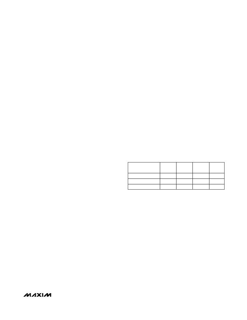
�Table� 2.� ADC� Default� Monitor� Full-Scale�
�Ranges�
�2)� Low� Transmit� Power� (LTXP)�
�3)� High� Transmit� Power� (HTXP)�
�4)� Max� Output� Current� (IBIASMAX)�
�5)� Loss-of-Signal� (LOS� LO)�
�The� high-transmit� and� low-transmit� power� quick-trip�
�SIGNAL�
�Temperature� (°C)�
�V� CC� (V)�
�MON1� –MON4� (V)�
�+FS�
�SIGNAL�
�127.996�
�6.5528�
�2.4997�
�+FS�
�hex�
�7FFF�
�FFF8�
�FFF8�
�-FS�
�SIGNAL�
�-128�
�0�
�0�
�-FS�
�hex�
�8000�
�0000�
�0000�
�registers� (HTXP� and� LTXP)� set� the� thresholds� used� to�
�compare� against� the� MON2� voltage� to� determine� if� the�
�transmit� power� is� within� specification.� The� HBATH�
�quick� trip� compares� the� MON1� input� (generally� from� the�
�laser� driver’s� bias� monitor� output)� against� its� threshold�
�setting� to� determine� if� the� present� bias� current� is� above�
�specification.� The� BIAS� MAX� quick� trip� determines� if� the�
�BIAS� DAC� is� above� specification� (IBIASMAX).� When� the�
�new� BIAS� DAC� value� is� calculated,� it� is� compared�
�against� the� IBIASMAX� register.� The� BIAS� DAC� is� not�
�allowed� to� exceed� the� value� set� in� the� IBIASMAX� regis-�
�ter.� When� the� DS1873� detects� that� the� bias� is� at� the�
�limit,� it� sets� the� BIASMAX� status� bit� and� holds� the� BIAS�
�DAC� setting� at� the� IBIASMAX� level.� The� bias� and� power�
�quick� trips� are� routed� to� the� TXF� through� interrupt�
�masks� to� allow� combinations� of� these� alarms� to� be�
�used� to� trigger� these� outputs.� The� user� can� program� up�
�to� eight� different� temperature-indexed� threshold� levels�
�for� MON1� (Table� 02h,� Register� D1h).� The� LOS� LO� quick�
�trip� compares� the� MON3� input� against� its� threshold� set-�
�ting� to� determine� if� the� present� received� power� is� below�
�The� ADC� results� (after� right-shifting,� if� used)� are� com-�
�pared� to� the� alarm� and� warning� thresholds� after� each�
�conversion,� and� the� corresponding� alarms� are� set,�
�which� can� be� used� to� trigger� the� TXF� output.� These�
�ADC� thresholds� are� user� programmable,� as� are� the�
�masking� registers� that� can� be� used� to� prevent� the�
�alarms� from� triggering� the� TXF� output.�
�ADC� Timing�
�There� are� six� analog� channels� that� are� digitized� in� a�
�round-robin� fashion� in� the� order� shown� in� Figure� 4.� The�
�total� time� required� to� convert� all� six� channels� is� t� RR� (see�
�the� Analog� Voltage� Monitoring� Characteristics� for�
�details).�
�Right-Shifting� ADC� Result�
�If� the� weighting� of� the� ADC� digital� reading� must� con-�
�form� to� a� predetermined� full-scale� (PFS)� value� defined�
�by� a� standard’s� specification� (e.g.,� SFF-8472),� then�
�right-shifting� can� be� used� to� adjust� the� PFS� analog�
�measurement� range� while� maintaining� the� weighting� of�
�______________________________________________________________________________________�
�15�
�相关PDF资料 |
PDF描述 |
|---|---|
| VE-24Z-CV-F3 | CONVERTER MOD DC/DC 2V 60W |
| ESM43DRTH | CONN EDGECARD 86POS DIP .156 SLD |
| DS1874T+T&R | IC CTLR SFP+ ANLG LDD 28-TQFN |
| HSC25DRAN-S734 | CONN EDGECARD 50POS .100 R/A PCB |
| HCC43DRTI-S93 | CONN EDGECARD 86POS DIP .100 SLD |
相关代理商/技术参数 |
参数描述 |
|---|---|
| DS1874 | 制造商:MAXIM 制造商全称:Maxim Integrated Products 功能描述:SFP+ Controller with Digital LDD Interface |
| DS1874T+ | 功能描述:ADC / DAC多通道 SFP+ Controller w/ Dgtl LDD Interface RoHS:否 制造商:Texas Instruments 转换速率: 分辨率:8 bit 接口类型:SPI 电压参考: 电源电压-最大:3.6 V 电源电压-最小:2 V 最大工作温度:+ 85 C 安装风格:SMD/SMT 封装 / 箱体:VQFN-40 |
| DS1874T+T&R | 制造商:Maxim Integrated Products 功能描述:SFP+ CONTROLLER WITH DIGITAL LDD INTERFACE - Tape and Reel 制造商:Maxim Integrated Products 功能描述:MXMDS1874T+T&R SFP+ CTRLR FOR USE W/MAX3 制造商:Maxim Integrated Products 功能描述:IC CTLR SFP+ ANLG LDD 28-TQFN |
| DS1874T+T&R | 功能描述:ADC / DAC多通道 SFP+ Controller w/ Dgtl LDD Interface RoHS:否 制造商:Texas Instruments 转换速率: 分辨率:8 bit 接口类型:SPI 电压参考: 电源电压-最大:3.6 V 电源电压-最小:2 V 最大工作温度:+ 85 C 安装风格:SMD/SMT 封装 / 箱体:VQFN-40 |
| DS1874T+TR | 制造商:MAXIM 制造商全称:Maxim Integrated Products 功能描述:SFP+ Controller with Digital LDD Interface |
发布紧急采购,3分钟左右您将得到回复。