- 您现在的位置:买卖IC网 > PDF目录20033 > DS1873T+T&R (Maxim Integrated)IC CTLR SFP+ ANLG LDD 28-TQFN PDF资料下载
参数资料
| 型号: | DS1873T+T&R |
| 厂商: | Maxim Integrated |
| 文件页数: | 16/86页 |
| 文件大小: | 0K |
| 描述: | IC CTLR SFP+ ANLG LDD 28-TQFN |
| 产品培训模块: | Lead (SnPb) Finish for COTS Obsolescence Mitigation Program |
| 标准包装: | 2,500 |
| 类型: | 激光二极管控制器 |
| 通道数: | 1 |
| 电源电压: | 2.85 V ~ 3.9 V |
| 电流 - 电源: | 2.5mA |
| 工作温度: | -40°C ~ 95°C |
| 封装/外壳: | 28-WFQFN 裸露焊盘 |
| 供应商设备封装: | 28-TQFN-EP(5x5) |
| 包装: | 带卷 (TR) |
| 安装类型: | 表面贴装 |
| 其它名称: | 90-1873T+TRL |
第1页第2页第3页第4页第5页第6页第7页第8页第9页第10页第11页第12页第13页第14页第15页当前第16页第17页第18页第19页第20页第21页第22页第23页第24页第25页第26页第27页第28页第29页第30页第31页第32页第33页第34页第35页第36页第37页第38页第39页第40页第41页第42页第43页第44页第45页第46页第47页第48页第49页第50页第51页第52页第53页第54页第55页第56页第57页第58页第59页第60页第61页第62页第63页第64页第65页第66页第67页第68页第69页第70页第71页第72页第73页第74页第75页第76页第77页第78页第79页第80页第81页第82页第83页第84页第85页第86页
�� �
�
�SFP+� Controller� with� Analog� LDD� Interface�
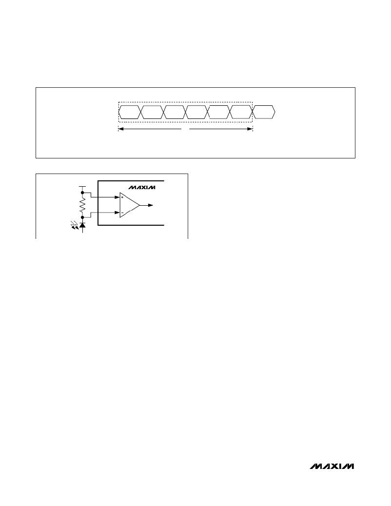
�ONE� ROUND-ROBIN� ADC� CYCLE�
�TEMP�
�V� CC�
�MON1�
�MON2�
�MON3�
�MON4�
�TEMP�
�t� RR�
�NOTE:� IF� THE� VCC� LO� ALARM� IS� ENABLED� AT� POWER-UP,� THE� ADC� ROUND-ROBIN� TIMING� CYCLES� BETWEEN� TEMPERATURE� AND� V� CC� ONLY� UNTIL� V� CC�
�IS� ABOVE� THE� V� CC� ALARM� LOW� THRESHOLD.�
�Figure� 4.� ADC� Round-Robin� Timing�
�Figure� 5.� This� reduces� board� complexity� by� eliminating�
�V� CC�
�the� need� for� a� high-side� differential� amplifier� or� a� cur-�
�MON3P�
�DS1873�
�rent� mirror.�
�100� Ω�
�MON3N�
�ADC�
�Enhanced� RSSI� Monitoring� (Dual-Range�
�Functionality)�
�The� DS1873� offers� a� feature� to� improve� the� accuracy�
�ROSA�
�Figure� 5.� MON3� Differential� Input� for� High-Side� RSSI�
�the� ADC� results.� The� DS1873’s� range� is� wide� enough� to�
�cover� all� requirements;� when� the� maximum� input� value�
�is� ≤� 1/2� of� the� FS� value,� right-shifting� can� be� used� to�
�obtain� greater� accuracy.� For� instance,� the� maximum�
�voltage� might� be� 1/8� the� specified� PFS� value,� so� only�
�1/8� the� converter’s� range� is� effective� over� this� range.�
�An� alternative� is� to� calibrate� the� ADC’s� full-scale� range�
�to� 1/8� the� readable� PFS� value� and� use� a� right-shift�
�value� of� 3.� With� this� implementation,� the� resolution� of�
�the� measurement� is� increased� by� a� factor� of� 8,� and�
�because� the� result� is� digitally� divided� by� 8� by� right-�
�shifting,� the� bit� weight� of� the� measurement� still� meets�
�the� standard’s� specification� (i.e.,� SFF-8472).�
�The� right-shift� operation� on� the� ADC� result� is� carried� out�
�based� on� the� contents� of� right-shift� control� registers�
�(Table� 02h,� Registers� 8Dh–8Fh)� in� EEPROM.� Four� ana-�
�log� channels,� MON1–MON4,� each� have� 3� bits� allocated�
�to� set� the� number� of� right-shifts.� Up� to� 7� right-shift� oper-�
�ations� are� allowed� and� are� executed� as� a� part� of� every�
�conversion� before� the� results� are� compared� to� the� high-�
�alarm� and� low-alarm� levels,� or� loaded� into� their� corre-�
�sponding� measurement� registers� (Lower� Memory,�
�Registers� 64h–6Bh).� This� is� true� during� the� setup� of�
�internal� calibration� as� well� as� during� subsequent� data�
�conversions.�
�Differential� MON3� Input�
�The� DS1873� offers� a� fully� differential� input� for� MON3.�
�This� enables� high-side� monitoring� of� RSSI,� as� shown� in�
�and� range� of� MON3,� which� is� most� commonly� used� for�
�monitoring� RSSI.� The� accuracy� of� the� RSSI� measure-�
�ments� is� increased� at� the� small� cost� of� reduced� range�
�(of� input� signal� swing).� The� DS1873� eliminates� this�
�trade-off� by� offering� “dual� range”� calibration� on� the�
�MON3� channel� (see� Figure� 5).� This� feature� enables�
�right-shifting� (along� with� its� gain� and� offset� settings)�
�when� the� input� signal� is� below� a� set� threshold� (within� the�
�range� that� benefits� using� right-shifting)� and� then� automat-�
�ically� disables� right-shifting� (recalling� different� gain� and�
�offset� settings)� when� the� input� signal� exceeds� the� thresh-�
�old.� Also,� to� prevent� “chattering,”� hysteresis� prevents�
�excessive� switching� between� modes� in� addition� to� ensur-�
�ing� that� continuity� is� maintained.� Dual-range� operation� is�
�enabled� by� default� (factory� programmed� in� EEPROM).�
�However,� it� can� easily� be� disabled� through� the� RSSI_FC�
�and� RSSI_FF� bits,� which� are� described� in� the� Register�
�Descriptions� section.� When� dual-range� operation� is� dis-�
�abled,� MON3� operates� identically� to� the� other� MON�
�channels,� although� featuring� a� differential� input.�
�Dual-range� functionality� consists� of� two� modes� of� opera-�
�tion:� fine� mode� and� coarse� mode.� Each� mode� is� calibrat-�
�ed� for� a� unique� transfer� function,� hence� the� term,� dual�
�range.� Table� 4� highlights� the� registers� related� to� MON3.�
�Fine� mode� is� equivalent� to� the� other� MON� channels.� Fine�
�mode� is� calibrated� using� the� gain,� offset,� and� right-shift-�
�ing� registers� at� locations� shown� in� Table� 4� and� is� ideal�
�for� relatively� small� analog� input� voltages.� Coarse� mode� is�
�automatically� switched� to� when� the� input� exceeds� a�
�threshold� (to� be� discussed� in� a� subsequent� paragraph).�
�Coarse� mode� is� calibrated� using� different� gain� and� offset�
�registers,� but� lacks� right-shifting� (since� coarse� mode� is�
�only� used� on� large� input� signals).� The� gain� and� offset�
�registers� for� coarse� mode� are� also� shown� in� Table� 4.�
�16�
�______________________________________________________________________________________�
�相关PDF资料 |
PDF描述 |
|---|---|
| VE-24Z-CV-F3 | CONVERTER MOD DC/DC 2V 60W |
| ESM43DRTH | CONN EDGECARD 86POS DIP .156 SLD |
| DS1874T+T&R | IC CTLR SFP+ ANLG LDD 28-TQFN |
| HSC25DRAN-S734 | CONN EDGECARD 50POS .100 R/A PCB |
| HCC43DRTI-S93 | CONN EDGECARD 86POS DIP .100 SLD |
相关代理商/技术参数 |
参数描述 |
|---|---|
| DS1874 | 制造商:MAXIM 制造商全称:Maxim Integrated Products 功能描述:SFP+ Controller with Digital LDD Interface |
| DS1874T+ | 功能描述:ADC / DAC多通道 SFP+ Controller w/ Dgtl LDD Interface RoHS:否 制造商:Texas Instruments 转换速率: 分辨率:8 bit 接口类型:SPI 电压参考: 电源电压-最大:3.6 V 电源电压-最小:2 V 最大工作温度:+ 85 C 安装风格:SMD/SMT 封装 / 箱体:VQFN-40 |
| DS1874T+T&R | 制造商:Maxim Integrated Products 功能描述:SFP+ CONTROLLER WITH DIGITAL LDD INTERFACE - Tape and Reel 制造商:Maxim Integrated Products 功能描述:MXMDS1874T+T&R SFP+ CTRLR FOR USE W/MAX3 制造商:Maxim Integrated Products 功能描述:IC CTLR SFP+ ANLG LDD 28-TQFN |
| DS1874T+T&R | 功能描述:ADC / DAC多通道 SFP+ Controller w/ Dgtl LDD Interface RoHS:否 制造商:Texas Instruments 转换速率: 分辨率:8 bit 接口类型:SPI 电压参考: 电源电压-最大:3.6 V 电源电压-最小:2 V 最大工作温度:+ 85 C 安装风格:SMD/SMT 封装 / 箱体:VQFN-40 |
| DS1874T+TR | 制造商:MAXIM 制造商全称:Maxim Integrated Products 功能描述:SFP+ Controller with Digital LDD Interface |
发布紧急采购,3分钟左右您将得到回复。