参数资料
| 型号: | DS21448 |
| 厂商: | Maxim Integrated Products |
| 文件页数: | 28/60页 |
| 文件大小: | 0K |
| 描述: | IC LIU QUAD E1/T1/J1 144-BGA |
| 产品培训模块: | Lead (SnPb) Finish for COTS Obsolescence Mitigation Program |
| 标准包装: | 1 |
| 类型: | 线路接口装置(LIU) |
| 驱动器/接收器数: | 4/4 |
| 规程: | T1/E1/J1 |
| 电源电压: | 3.135 V ~ 3.465 V |
| 安装类型: | 表面贴装 |
| 封装/外壳: | 144-BGA |
| 供应商设备封装: | 144-TEPBGA(17x17) |
| 包装: | 管件 |
第1页第2页第3页第4页第5页第6页第7页第8页第9页第10页第11页第12页第13页第14页第15页第16页第17页第18页第19页第20页第21页第22页第23页第24页第25页第26页第27页当前第28页第29页第30页第31页第32页第33页第34页第35页第36页第37页第38页第39页第40页第41页第42页第43页第44页第45页第46页第47页第48页第49页第50页第51页第52页第53页第54页第55页第56页第57页第58页第59页第60页
DS21448 3.3V T1/E1/J1 Quad Line Interface
34 of 60
10Hz to 100kHz) is added to the jitter present on TCLK. Also, the waveforms created are independent of the duty
cycle of TCLK. The transmitter couples to the E1 or T1 transmit-twisted pair (or coaxial cable in some E1
applications) through a 1:2 step-up transformer. For the device to create the proper waveforms, the transformer
used must meet the specifications listed in Table 7-C.
The DS21448 has an automatic short-circuit limiter that limits the source current to 50mA (RMS) into a 1 load.
This feature can be disabled by setting the SCLD bit (CCR2.5) = 1. When the current limiter is activated, TCLE
(SR.2) is set even if the short-circuit limiter is disabled. The TPD bit (CCR4.0) powers down the transmit-line driver
and tri-states the TTIP and TRING pins. The DS21448 can also detect when the TTIP or TRING outputs are open
circuited. When an open circuit is detected, TOCD (SR.1) is set.
7.3 Jitter Attenuator
The DS21448 contains an on-board jitter attenuator that can be set to a depth of either 32 or 128 bits through the
JABDS bit (CCR4.2). The 128-bit mode is used in applications where large excursions of wander are expected.
The 32-bit mode is used in delay-sensitive applications. Figure 7-8 shows the attenuation characteristics. The jitter
attenuator can be placed in either the receive path or the transmit path by appropriately setting or clearing the JAS
bit (CCR4.3). Also, setting the DJA bit (CCR4.1) can disable the jitter attenuator (in effect, remove it). For the jitter
attenuator to operate properly, a 2.048MHz or 1.544MHz clock must be applied at MCLK. ITU specification G.703
requires ±50ppm accuracy for T1 and E1. TR62411 and ANSI specs require ±32ppm accuracy for T1 interfaces.
An on-board PLL for the jitter attenuator converts the 2.048MHz clock to a 1.544MHz rate for T1 applications.
Setting JAMUX (CCR1.3) to logic 0 bypasses this PLL. On-board circuitry adjusts either the recovered clock from
the clock/data recovery block or the clock applied at the TCLK pin to create a smooth jitter-free clock, which is used
to clock data out of the jitter attenuator FIFO. It is acceptable to provide a gapped/bursty clock at the TCLK pin if
the jitter attenuator is placed on the transmit side. If the incoming jitter exceeds either 120UIP-P (buffer depth is 128
bits) or 28UIP-P (buffer depth is 32 bits), the DS21448 divides the internal nominal 32.768MHz (E1) or 24.704MHz
(T1) clock by either 15 or 17 instead of the normal 16 to keep the buffer from overflowing. When the device divides
by either 15 or 17, it also sets the JALT bit in the receive information register 1 (RIR1).
7.4 G.703 Synchronization Signal
The DS21448 can receive a 2.048MHz square-wave synchronization clock, as specified in Section 10 of ITU
G.703. To use the DS21448 in this mode, set the receive-synchronization-clock enable (CCR5.3) = 1. The
DS21448 can also transmit the 2.048MHz square-wave synchronization clock, as specified in Section 10 of G.703.
To transmit the 2.048MHz clock, set the transmit-synchronization-clock enable (CCR5.2) = 1.
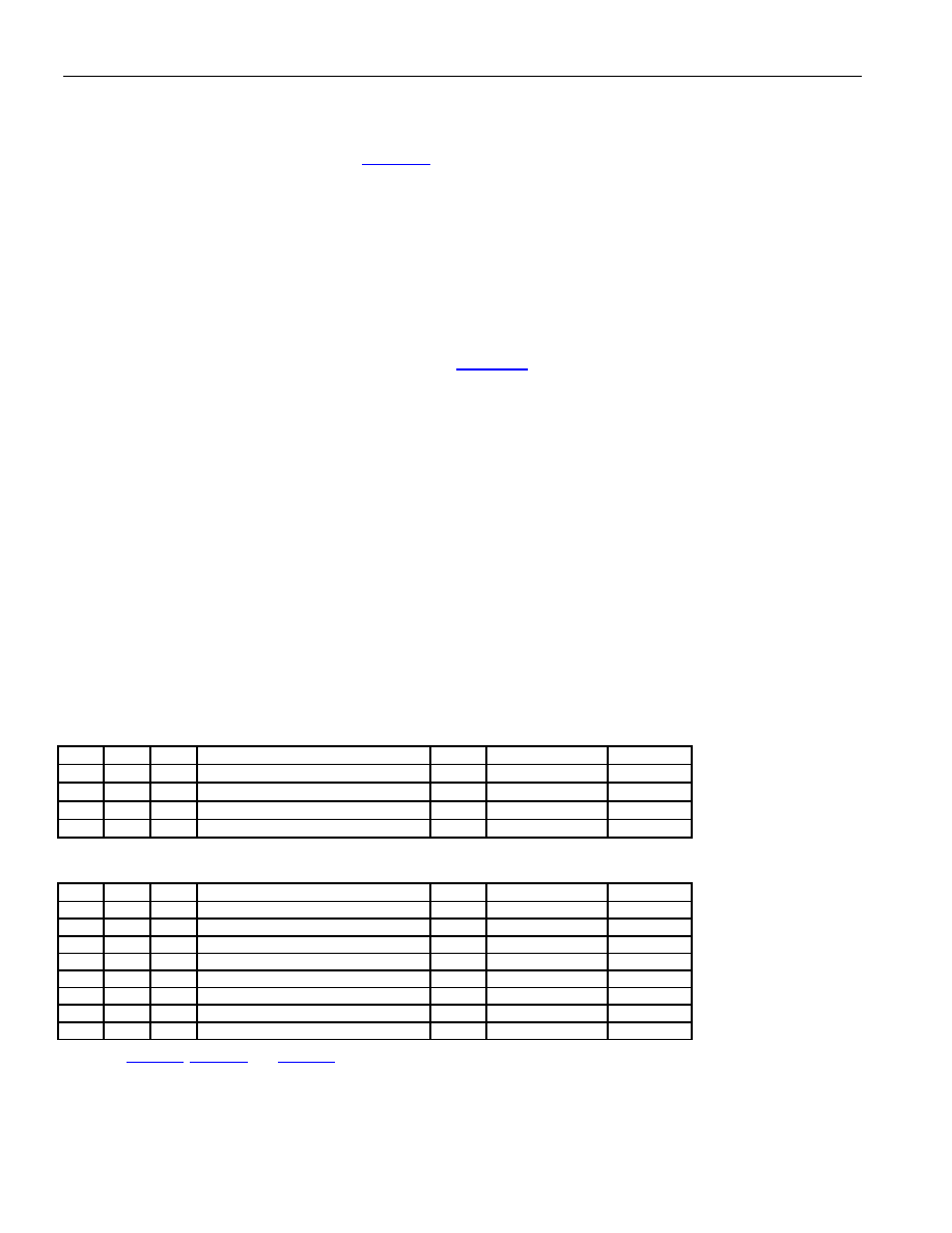
Table 7-A. Line Build-Out Select for E1 in Register CCR4 (ETS = 0)
L2
L1
L0
APPLICATION
N
RETURN LOSS
Rt ()
0
75
normal
1:2
N.M.
0
1
120
normal
1:2
N.M.
0
1
0
75
with high return loss
1:2
21dB
6.2
1
0
1
120
with high return loss
1:2
21dB
11.6
Table 7-B. Line Build-Out Select for T1 in Register CCR4 (ETS = 1)
L2
L1
L0
APPLICATION
N
RETURN LOSS
Rt ()
0
DSX-1 (0 to 133ft)/0dB CSU
1:2
N.M.
0
1
DSX-1 (133 to 266f)
1:2
N.M.
0
1
0
DSX-1 (266 to 399ft)
1:2
N.M.
0
1
DSX-1 (399 to 533ft)
1:2
N.M.
0
1
0
DSX-1 (533 to 655ft)
1:2
N.M.
0
1
0
1
-7.5dB CSU
1:2
N.M.
0
1
0
-15dB CSU
1:2
N.M.
0
1
-22.5dB CSU
1:2
N.M.
0
N.M. = Not meaningful.
相关PDF资料 |
PDF描述 |
|---|---|
| DS3151N+ | IC LIU DS3/E3/STS-1 144CSBGA |
| VI-24L-MX-F3 | CONVERTER MOD DC/DC 28V 75W |
| D38999/24JB5HN | CONN RCPT 5POS JAM NUT W/PINS |
| VI-24L-MX-F2 | CONVERTER MOD DC/DC 28V 75W |
| HI7191IB | IC ADC 24BIT PROGBL SER 20-SOIC |
相关代理商/技术参数 |
参数描述 |
|---|---|
| DS21448A1 | 功能描述:网络控制器与处理器 IC 3.3V E1/T1/J1 Quad Interface RoHS:否 制造商:Micrel 产品:Controller Area Network (CAN) 收发器数量: 数据速率: 电源电流(最大值):595 mA 最大工作温度:+ 85 C 安装风格:SMD/SMT 封装 / 箱体:PBGA-400 封装:Tray |
| DS21448DK | 功能描述:网络开发工具 DS21448 Dev Kit RoHS:否 制造商:Rabbit Semiconductor 产品:Development Kits 类型:Ethernet to Wi-Fi Bridges 工具用于评估:RCM6600W 数据速率:20 Mbps, 40 Mbps 接口类型:802.11 b/g, Ethernet 工作电源电压:3.3 V |
| DS21448G+ | 功能描述:网络控制器与处理器 IC 3.3V E1/T1/J1 Quad Interface RoHS:否 制造商:Micrel 产品:Controller Area Network (CAN) 收发器数量: 数据速率: 电源电流(最大值):595 mA 最大工作温度:+ 85 C 安装风格:SMD/SMT 封装 / 箱体:PBGA-400 封装:Tray |
| DS21448GN+ | 功能描述:网络控制器与处理器 IC 3.3V E1/T1/J1 Quad Interface RoHS:否 制造商:Micrel 产品:Controller Area Network (CAN) 收发器数量: 数据速率: 电源电流(最大值):595 mA 最大工作温度:+ 85 C 安装风格:SMD/SMT 封装 / 箱体:PBGA-400 封装:Tray |
| DS21448L | 功能描述:网络控制器与处理器 IC 3.3V E1/T1/J1 Quad Interface RoHS:否 制造商:Micrel 产品:Controller Area Network (CAN) 收发器数量: 数据速率: 电源电流(最大值):595 mA 最大工作温度:+ 85 C 安装风格:SMD/SMT 封装 / 箱体:PBGA-400 封装:Tray |
发布紧急采购,3分钟左右您将得到回复。