- 您现在的位置:买卖IC网 > PDF目录15727 > DS21448LDK (Maxim Integrated Products)KIT DESIGN LIU DS21448L T1/J1/E1 PDF资料下载
参数资料
| 型号: | DS21448LDK |
| 厂商: | Maxim Integrated Products |
| 文件页数: | 14/60页 |
| 文件大小: | 0K |
| 描述: | KIT DESIGN LIU DS21448L T1/J1/E1 |
| 标准包装: | 1 |
第1页第2页第3页第4页第5页第6页第7页第8页第9页第10页第11页第12页第13页当前第14页第15页第16页第17页第18页第19页第20页第21页第22页第23页第24页第25页第26页第27页第28页第29页第30页第31页第32页第33页第34页第35页第36页第37页第38页第39页第40页第41页第42页第43页第44页第45页第46页第47页第48页第49页第50页第51页第52页第53页第54页第55页第56页第57页第58页第59页第60页
DS21448 3.3V T1/E1/J1 Quad Line Interface
21 of 60
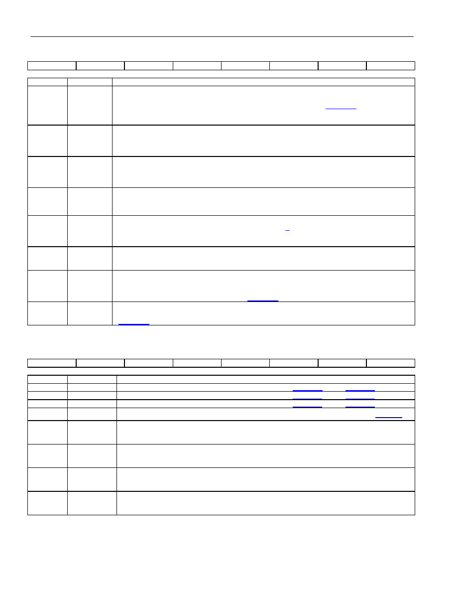
CCR3 (02H): Common Control Register 3
(MSB)
(LSB)
TUA1
ATUA1
TAOZ
TPRBSE
TLCE
LIRST
IBPV
IBE
NAME
POSITION
FUNCTION
TUA1
CCR3.7
Transmit Unframed All Ones. The polarity of this bit is set such that the device transmits an all-
ones pattern on power-up or device reset. This bit must be set to 1 to allow the device to transmit
data. The transmission of this data pattern is always timed off JACLK (Figure 1-1).
0 = transmit all ones at TTIP and TRING
1 = transmit data normally
ATUA1
CCR3.6
Automatic Transmit Unframed All Ones. Automatically transmit an unframed all-ones pattern at
TTIP and TRING during an RCL condition.
0 = disabled
1 = enabled
TAOZ
CCR3.5
Transmit Alternate Ones and Zeros. Transmit a …101010… pattern at TTIP and TRING. The
transmission of this data pattern is always timed off TCLK.
0 = disabled
1 = enabled
TPRBSE
CCR3.4
Transmit PRBS Enable. Transmit a 2
15 - 1 (E1) or a QRSS (T1) PRBS at TTIP and TRING.
0 = disabled
1 = enabled
TLCE
CCR3.3
Transmit Loop-Code Enable. Enables the transmit side to transmit the loop-up code in the transmit
code definition registers (TCD1 and TCD2). See Section 6 for details.
0 = disabled
1 = enabled
LIRST
CCR3.2
Line Interface Reset. Setting this bit from 0 to 1 initiates an internal reset that resets the clock
recovery state machine and recenters the jitter attenuator. Normally this bit is only toggled on
power-up. It must be cleared and set again for a subsequent reset.
IBPV
CCR3.1
Insert Bipolar Violation (BPV). A 0-to-1 transition on this bit causes a single bipolar violation to be
inserted into the transmit data stream. Once this bit has been toggled from 0 to 1, the device waits
for the next occurrence of three consecutive 1s to insert the BPV. This bit must be cleared and set
again for a subsequent error to be inserted (Figure 1-3).
IBE
CCR3.0
Insert Bit Error. A 0-to-1 transition on this bit causes a single logic error to be inserted into the
transmit data stream. This bit must be cleared and set again for a subsequent error to be inserted
CCR4 (03H): Common Control Register 4
(MSB)
(LSB)
L2
L1
L0
EGL
JAS
JABDS
DJA
TPD
NAME
POSITION
FUNCTION
L2
CCR4.7
Line Build-Out Select Bit 2. Sets the transmitter build-out (Table 7-A for E1, Table 7-B for T1).
L1
CCR4.6
Line Build Out Select Bit 1. Sets the transmitter build-out (Table 7-A for E1, Table 7-B for T1).
L0
CCR4.5
Line Build Out Select Bit 0. Sets the transmitter build-out (Table 7-A for E1, Table 7-B for T1).
EGL
CCR4.4
Receive Equalizer Gain Limit. This bit controls the sensitivity of the receive equalizer (Table 4-I).
JAS
CCR4.3
Jitter Attenuator Path Select
0 = place the jitter attenuator on the receive side
1 = place the jitter attenuator on the transmit side
JABDS
CCR4.2
Jitter Attenuator Buffer Depth Select
0 = 128 bits
1 = 32 bits (use for delay-sensitive applications)
DJA
CCR4.1
Disable Jitter Attenuator
0 = jitter attenuator enabled
1 = jitter attenuator disabled
TPD
CCR4.0
Transmit Power-Down
0 = normal transmitter operation
1 = powers down the transmitter and tri-states the TTIP and TRING pins
相关PDF资料 |
PDF描述 |
|---|---|
| SRR1005-561K | INDUCTOR 560UH 280MA SMD |
| CDH53NP-330KC | POWER INDUCTOR 33UH 0.67A SMD |
| CDH53NP-2R2MC | POWER INDUCTOR 2.2UH 2.03A SMD |
| CDH53NP-270KC | POWER INDUCTOR 27UH 0.72A SMD |
| CDH53NP-221JC | POWER INDUCTOR 220UH 0.26A SMD |
相关代理商/技术参数 |
参数描述 |
|---|---|
| DS21448LN | 功能描述:网络控制器与处理器 IC 3.3V E1/T1/J1 Quad Interface RoHS:否 制造商:Micrel 产品:Controller Area Network (CAN) 收发器数量: 数据速率: 电源电流(最大值):595 mA 最大工作温度:+ 85 C 安装风格:SMD/SMT 封装 / 箱体:PBGA-400 封装:Tray |
| DS21448LN+ | 功能描述:网络控制器与处理器 IC 3.3V E1/T1/J1 Quad Interface RoHS:否 制造商:Micrel 产品:Controller Area Network (CAN) 收发器数量: 数据速率: 电源电流(最大值):595 mA 最大工作温度:+ 85 C 安装风格:SMD/SMT 封装 / 箱体:PBGA-400 封装:Tray |
| DS21448-LW | 功能描述:网络控制器与处理器 IC 3.3V E1/T1/J1 Quad Interface RoHS:否 制造商:Micrel 产品:Controller Area Network (CAN) 收发器数量: 数据速率: 电源电流(最大值):595 mA 最大工作温度:+ 85 C 安装风格:SMD/SMT 封装 / 箱体:PBGA-400 封装:Tray |
| DS21448N | 功能描述:网络控制器与处理器 IC 3.3V E1/T1/J1 Quad Interface RoHS:否 制造商:Micrel 产品:Controller Area Network (CAN) 收发器数量: 数据速率: 电源电流(最大值):595 mA 最大工作温度:+ 85 C 安装风格:SMD/SMT 封装 / 箱体:PBGA-400 封装:Tray |
| DS2145 | 制造商:未知厂家 制造商全称:未知厂家 功能描述:Telecommunication IC |
发布紧急采购,3分钟左右您将得到回复。