- 您现在的位置:买卖IC网 > PDF目录15727 > DS21448LDK (Maxim Integrated Products)KIT DESIGN LIU DS21448L T1/J1/E1 PDF资料下载
参数资料
| 型号: | DS21448LDK |
| 厂商: | Maxim Integrated Products |
| 文件页数: | 4/60页 |
| 文件大小: | 0K |
| 描述: | KIT DESIGN LIU DS21448L T1/J1/E1 |
| 标准包装: | 1 |
第1页第2页第3页当前第4页第5页第6页第7页第8页第9页第10页第11页第12页第13页第14页第15页第16页第17页第18页第19页第20页第21页第22页第23页第24页第25页第26页第27页第28页第29页第30页第31页第32页第33页第34页第35页第36页第37页第38页第39页第40页第41页第42页第43页第44页第45页第46页第47页第48页第49页第50页第51页第52页第53页第54页第55页第56页第57页第58页第59页第60页
DS21448 3.3V T1/E1/J1 Quad Line Interface
12 of 60
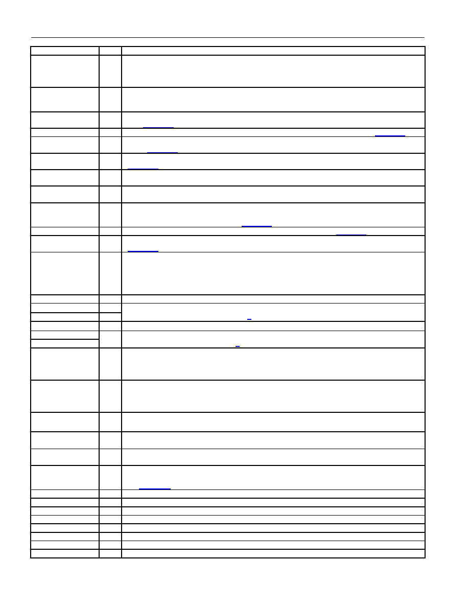
PIN
I/O
FUNCTION
CES
I
Receive and Transmit Clock Select. Selects which RCLK edge to update RPOS and RNEG and
which TCLK edge to sample TPOS and TNEG. CES combines TCES and RCES.
0 = update RPOS/RNEG on rising edge of RCLK; sample TPOS/TNEG on falling edge of TCLK
1 = update RPOS/RNEG on falling edge of RCLK; sample TPOS/TNEG on rising edge of TCLK
TPD
I
Transmit Power-Down
0 = normal transmitter operation
1 = powers down the transmitter and tri-states TTIP and TRING pins
TX0/TX1
I
Transmit Data Source Select Bits 0 and 1. These inputs determine the source of the transmit
data (Table 4-B).
LOOP0/LOOP1
I
Loopback Select Bits 0 and 1. These inputs determine the active loopback mode (Table 4-A).
MM0/MM1
I
Monitor Mode Select Bits 0 and 1. These inputs determine if the receive equalizer is in a monitor
mode (Table 4-D).
RT1/RT0
I
Receive LIU Termination Select Bits 0 and 1. These inputs determine the receive termination
TEST
I
Tri-State Control. Set high to tri-state all outputs and I/O pins (including the parallel control port).
Set low for normal operation. Useful in board-level testing.
HRST
I
Hardware Reset. Bringing
HRST low resets the DS21448, setting all control bits to the all-zero
default state.
MCLK
I
Master Clock. A 2.048MHz (±50ppm) clock source with TTL levels is applied at this pin. This
clock is used internally for both clock/data recovery and for jitter attenuation. A T1 1.544MHz
clock source is optional (Note 1). See Table 4-F for details.
BIS0/BIS1
I
Bus Interface Select Bit 0 and 1. Used to select bus interface option (Table 2-A).
EGL1–EGL4
I
Receive Equalizer Gain-Limit Select. These bits control the sensitivity of the receive equalizers
PBEO1–PBEO4
O
PRBS Bit-Error Output. The receiver constantly searches for a 2
15 - 1 PRBS (ETS = 0) or a
QRSS PRBS (ETS = 1). The pattern is chosen automatically by the value of the ETS pin. It
remains high if it is out of synchronization with the PRBS pattern. It goes low when synchronized
to the PRBS pattern. Any errors in the received pattern after synchronization cause a positive-
going pulse (with same period as E1 or T1 clock) synchronous with RCLK.
RCL1–RCL4
O
Receive Carrier Loss. An output that toggles high during a receive carrier loss.
RTIP1–RTIP4
I
RRING1–RRING4
I
Receive Tip and Ring. Analog inputs for clock recovery circuitry. These pins connect through a
1:1 transformer to the line. See Section 7 for details.
BPCLK1–BPCLK4
O
Backplane Clock. A 16.384MHz clock output that is referenced to RCLK.
TTIP1–TTIP4
TRING1–TRING4
O
Transmit Tip and Ring. Analog line-driver outputs. These pins connect through a step-up
transformer to the line. See Section 7 for details.
RPOS1–RPOS4
O
Receive Positive Data. Updated on the rising edge (CES = 0) or the falling edge (CES = 1) of
RCLK with bipolar data out of the line interface. In NRZ mode (NRZE = 1), data is output on
RPOS, and a received error (BPV, CV, or EXZ) causes a positive-going pulse synchronous with
RCLK at RNEG.
RNEG1–RNEG4
O
Receive Negative Data. Updated on the rising edge (CES = 0) or the falling edge (CES = 1) of
RCLK with bipolar data out of the line interface. In NRZ mode (NRZE = 1), data is output on
RPOS, and a received error (BPV, CV, or EXZ) causes a positive-going pulse synchronous with
RCLK at RNEG.
RCLK1–RCLK4
O
Receive Clock. Buffered recovered clock from the line. Synchronous to MCLK in absence of
signal at RTIP and RRING.
TPOS1–TPOS4
I
Transmit Positive Data. Sampled on the falling edge (CES = 0) or the rising edge (CES = 1) of
TCLK for data to be transmitted out onto the line.
TNEG1–TNEG4
I
Transmit Negative Data. Sampled on the falling edge (CES = 0) or the rising edge (CES = 1) of
TCLK for data to be transmitted out onto the line.
TCLK1–TCLK4
I
Transmit Clock. A 2.048MHz or 1.544MHz primary clock used to clock data through the transmit
side formatter. It can be sourced internally by MCLK or RCLK. See Common Control Register 1
and Figure 1-3.
JTRST
I
JTAG Reset
JTMS
I
JTAG Mode Select
JTCLK
I
JTAG Clock
JTDI
I
JTAG Data In
JTDO
O
JTAG Data Out
VSM
I
Voltage Supply Mode (LQFP only). VSM should be wired low for correct operation.
TVDD1–TVDD4
–
3.3V, ±5% Transmitter Positive Supply
VDD1–VDD4
—
3.3V, ±5% Positive Supply
相关PDF资料 |
PDF描述 |
|---|---|
| SRR1005-561K | INDUCTOR 560UH 280MA SMD |
| CDH53NP-330KC | POWER INDUCTOR 33UH 0.67A SMD |
| CDH53NP-2R2MC | POWER INDUCTOR 2.2UH 2.03A SMD |
| CDH53NP-270KC | POWER INDUCTOR 27UH 0.72A SMD |
| CDH53NP-221JC | POWER INDUCTOR 220UH 0.26A SMD |
相关代理商/技术参数 |
参数描述 |
|---|---|
| DS21448LN | 功能描述:网络控制器与处理器 IC 3.3V E1/T1/J1 Quad Interface RoHS:否 制造商:Micrel 产品:Controller Area Network (CAN) 收发器数量: 数据速率: 电源电流(最大值):595 mA 最大工作温度:+ 85 C 安装风格:SMD/SMT 封装 / 箱体:PBGA-400 封装:Tray |
| DS21448LN+ | 功能描述:网络控制器与处理器 IC 3.3V E1/T1/J1 Quad Interface RoHS:否 制造商:Micrel 产品:Controller Area Network (CAN) 收发器数量: 数据速率: 电源电流(最大值):595 mA 最大工作温度:+ 85 C 安装风格:SMD/SMT 封装 / 箱体:PBGA-400 封装:Tray |
| DS21448-LW | 功能描述:网络控制器与处理器 IC 3.3V E1/T1/J1 Quad Interface RoHS:否 制造商:Micrel 产品:Controller Area Network (CAN) 收发器数量: 数据速率: 电源电流(最大值):595 mA 最大工作温度:+ 85 C 安装风格:SMD/SMT 封装 / 箱体:PBGA-400 封装:Tray |
| DS21448N | 功能描述:网络控制器与处理器 IC 3.3V E1/T1/J1 Quad Interface RoHS:否 制造商:Micrel 产品:Controller Area Network (CAN) 收发器数量: 数据速率: 电源电流(最大值):595 mA 最大工作温度:+ 85 C 安装风格:SMD/SMT 封装 / 箱体:PBGA-400 封装:Tray |
| DS2145 | 制造商:未知厂家 制造商全称:未知厂家 功能描述:Telecommunication IC |
发布紧急采购,3分钟左右您将得到回复。