- 您现在的位置:买卖IC网 > PDF目录15727 > DS21448LDK (Maxim Integrated Products)KIT DESIGN LIU DS21448L T1/J1/E1 PDF资料下载
参数资料
| 型号: | DS21448LDK |
| 厂商: | Maxim Integrated Products |
| 文件页数: | 5/60页 |
| 文件大小: | 0K |
| 描述: | KIT DESIGN LIU DS21448L T1/J1/E1 |
| 标准包装: | 1 |
第1页第2页第3页第4页当前第5页第6页第7页第8页第9页第10页第11页第12页第13页第14页第15页第16页第17页第18页第19页第20页第21页第22页第23页第24页第25页第26页第27页第28页第29页第30页第31页第32页第33页第34页第35页第36页第37页第38页第39页第40页第41页第42页第43页第44页第45页第46页第47页第48页第49页第50页第51页第52页第53页第54页第55页第56页第57页第58页第59页第60页
DS21448 3.3V T1/E1/J1 Quad Line Interface
13 of 60
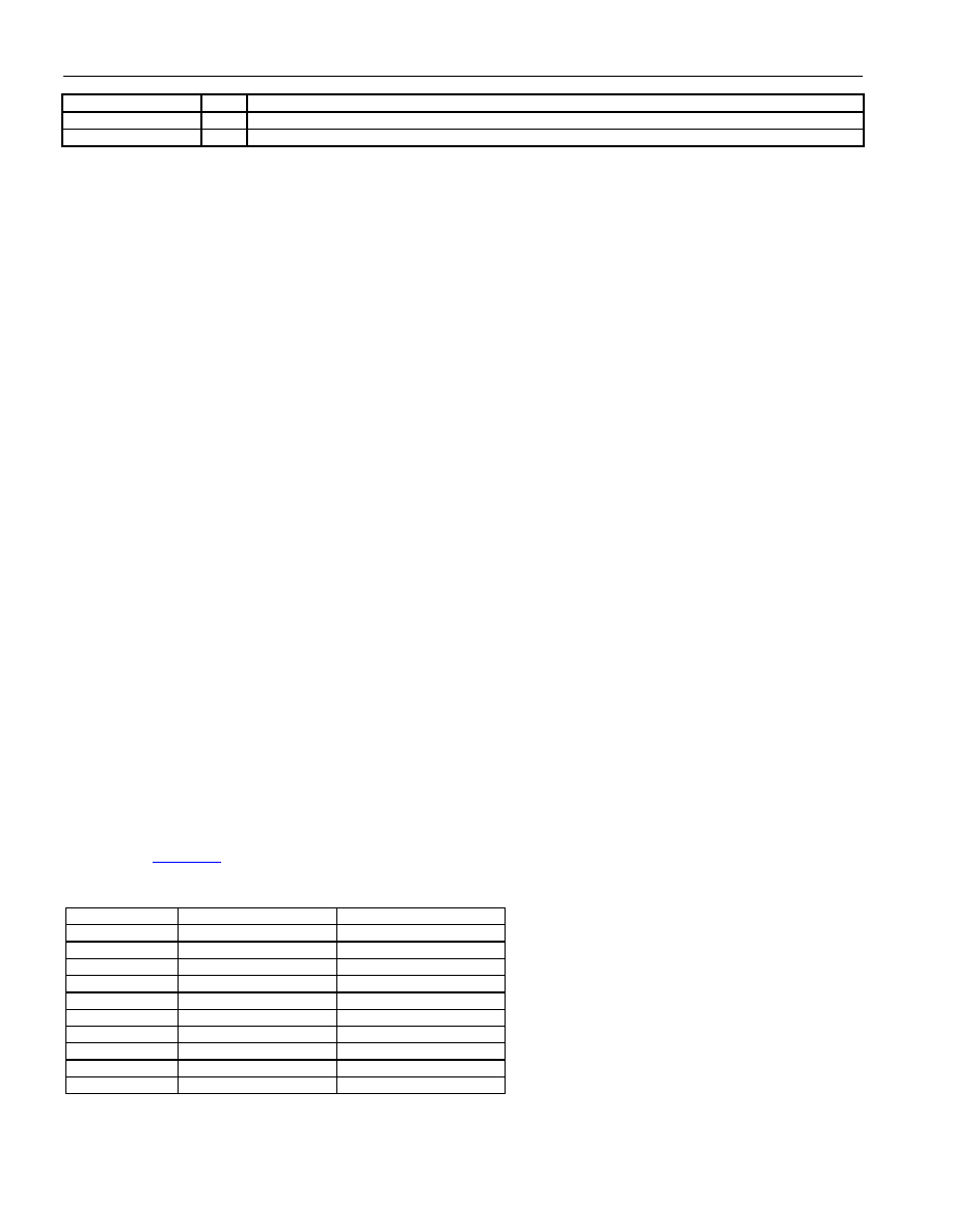
PIN
I/O
FUNCTION
TVSS1–TVSS4
—
Transmitter Signal Ground for Transmitter Outputs
VSS1–VSS4
—
Signal Ground
Note 1: G.703 requires an accuracy of ±50ppm for T1 and E1. TR62411 and ANSI specs require ±32ppm accuracy for T1 interfaces.
3. DETAILED DESCRIPTION
The DS21448 has a usable receiver sensitivity of 0 to -43dB for E1 applications and 0 to -36dB for T1 that allows it
to operate on 0.63mm (22AWG) cables up to 2.5km (E1) and 6000ft (T1) in length. The user has the option to use
internal receive termination, software selectable for 75
, 100, and 120 applications, or external termination.
The on-board crystal-less jitter attenuator can be placed in either the transmit or the receive data path, and requires
only a 2.048MHz MCLK for both E1 and T1 applications (with the option of using a 1.544MHz MCLK in T1
applications).
The DS21448 has diagnostic capabilities such as loopbacks and PRBS pattern generation and detection. 16-bit
loop-up and loop-down codes can be generated and detected. A single input pin can power down all transmitters to
allow the implementation of hitless protection switching (HPS) for 1+1 redundancy without the use of relays. The
device can be controlled through an 8-bit parallel port (muxed or nonmuxed) or a serial port, and it can be used in
hardware mode. A standard boundary scan interface supports board-level testing.
The DS21448 contains four independent LIUs that share a common interface for configuration and status. The user
can choose between three different means of accessing the device: a parallel microprocessor interface, a serial
interface, and a hardwired mode, which configures the device by setting levels on the device’s pins. The
DS21448’s four chip selects (
CS1, CS2, CS3, and CS4) determine which LIU is accessed when using the parallel
or serial interface modes. Four sets of identical register maps exist, one for each channel. Using the appropriate
chip select accesses a channel’s register map.
The analog AMI/HDB3 waveform off the E1 line or the AMI/B8ZS waveform off the T1 line is transformer-coupled
into the RTIP and RRING pins of the DS21448. The user has the option to use internal termination, software
selectable for 75
/100/120 applications, or external termination. The device recovers clock and data from the
analog signal and passes it through the jitter attenuation mux, outputting the received line clock at RCLK and
bipolar or NRZ data at RPOS and RNEG. The DS21448 contains an active filter that reconstructs the analog-
received signal for the nonlinear losses that occur in transmission. The receive circuitry is also configurable for
various monitor applications. The device has a usable receive sensitivity of 0 to -43dB for E1 and 0 to -36dB for T1
that allows the device to operate on 0.63mm (22AWG) cables up to 2.5km (E1) and 6k feet (T1) in length. Data
input at TPOS and TNEG is sent through the jitter attenuation mux to the waveshaping circuitry and line driver. The
DS21448 drives the E1 or T1 line from the TTIP and TRING pins through a coupling transformer. The line driver
can handle both CEPT 30/ISDN-PRI lines for E1 and long-haul (CSU) or short-haul (DSX-1) lines for T1.
3.1 DS21448 and DS21Q348 Differences
The DS21448 BGA is a monolithic quad-port LIU that is a replacement for the DS21Q348. The additional features
of JTAG, transmit driver disable, and the serial interface in the DS21448 have changed the function of several pins,
as shown in Table 3-A.
Table 3-A. DS21448 vs. DS21Q348 Pin Differences
PIN
DS21Q348
DS21448
G4
VSM
N.C.
J1
VSS
SCLK
K1
A4
A4/SDO
K3
VSS
SDI
K7
TEST
TXDIS/TEST
L3
N.C.
JTRST*
M3
N.C.
JTMS*
M5
N.C.
JTCLK
M6
N.C.
JTDI*
M7
N.C.
JTDO
*DS21448 pin is internally pulled up.
相关PDF资料 |
PDF描述 |
|---|---|
| SRR1005-561K | INDUCTOR 560UH 280MA SMD |
| CDH53NP-330KC | POWER INDUCTOR 33UH 0.67A SMD |
| CDH53NP-2R2MC | POWER INDUCTOR 2.2UH 2.03A SMD |
| CDH53NP-270KC | POWER INDUCTOR 27UH 0.72A SMD |
| CDH53NP-221JC | POWER INDUCTOR 220UH 0.26A SMD |
相关代理商/技术参数 |
参数描述 |
|---|---|
| DS21448LN | 功能描述:网络控制器与处理器 IC 3.3V E1/T1/J1 Quad Interface RoHS:否 制造商:Micrel 产品:Controller Area Network (CAN) 收发器数量: 数据速率: 电源电流(最大值):595 mA 最大工作温度:+ 85 C 安装风格:SMD/SMT 封装 / 箱体:PBGA-400 封装:Tray |
| DS21448LN+ | 功能描述:网络控制器与处理器 IC 3.3V E1/T1/J1 Quad Interface RoHS:否 制造商:Micrel 产品:Controller Area Network (CAN) 收发器数量: 数据速率: 电源电流(最大值):595 mA 最大工作温度:+ 85 C 安装风格:SMD/SMT 封装 / 箱体:PBGA-400 封装:Tray |
| DS21448-LW | 功能描述:网络控制器与处理器 IC 3.3V E1/T1/J1 Quad Interface RoHS:否 制造商:Micrel 产品:Controller Area Network (CAN) 收发器数量: 数据速率: 电源电流(最大值):595 mA 最大工作温度:+ 85 C 安装风格:SMD/SMT 封装 / 箱体:PBGA-400 封装:Tray |
| DS21448N | 功能描述:网络控制器与处理器 IC 3.3V E1/T1/J1 Quad Interface RoHS:否 制造商:Micrel 产品:Controller Area Network (CAN) 收发器数量: 数据速率: 电源电流(最大值):595 mA 最大工作温度:+ 85 C 安装风格:SMD/SMT 封装 / 箱体:PBGA-400 封装:Tray |
| DS2145 | 制造商:未知厂家 制造商全称:未知厂家 功能描述:Telecommunication IC |
发布紧急采购,3分钟左右您将得到回复。