参数资料
| 型号: | DS2149QN+ |
| 厂商: | Maxim Integrated Products |
| 文件页数: | 14/32页 |
| 文件大小: | 0K |
| 描述: | IC LIU T1/J1 5V 28-PLCC |
| 产品培训模块: | Lead (SnPb) Finish for COTS Obsolescence Mitigation Program |
| 标准包装: | 37 |
| 类型: | 线路接口装置(LIU) |
| 规程: | T1/J1 |
| 电源电压: | 4.75 V ~ 5.25 V |
| 安装类型: | 表面贴装 |
| 封装/外壳: | 28-LCC(J 形引线) |
| 供应商设备封装: | 28-PLCC(11.51x11.51) |
| 包装: | 管件 |
第1页第2页第3页第4页第5页第6页第7页第8页第9页第10页第11页第12页第13页当前第14页第15页第16页第17页第18页第19页第20页第21页第22页第23页第24页第25页第26页第27页第28页第29页第30页第31页第32页
DS2149
21 of 32
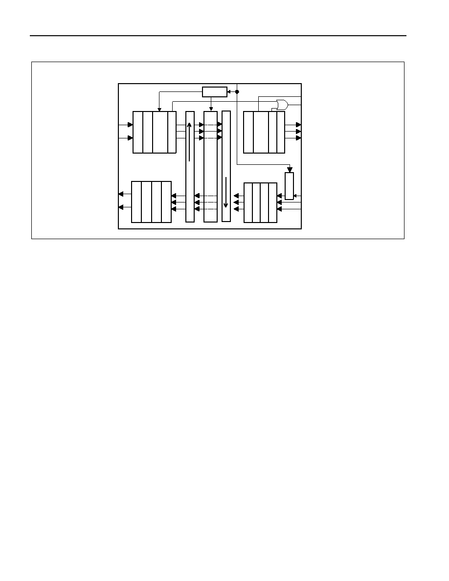
Figure 10-1. Loopbacks in the DS2149 Block Diagram
10.2Internal Pattern Generation and Detection
10.2.1 Transmit Alarm-Indication Signal (TAIS)
When TAIS is enabled (set TAIS in CR2, or pulling the TAIS pin high), the transmitter inputs
TPOS/TNEG and TDATA are ignored and the devices transmits unframed all ones at the transmitter
outputs at the TCLK frequency. If TCLK is not present, then the device uses MCLK to transmit. Both
TAIS and LLB can be enabled at the same time. The transmitter input data is looped back to the receiver
outputs through the jitter attenuator if enabled and the unframed all ones pattern is transmitted at TTIP
and TRING.
10.2.2 Quasirandom Signal Source (QRSS)
The QRSS data pattern is described in AT&T 62411. The pattern is represented by the polynomial 220- 1
with the additional requirement that no more than 14 consecutive 0s be present in the pattern. When
QRSS is enabled (PAT0 = 0 and PAT1 = 1 in CR2 or float the QRSS pin), the data at the transmitter
inputs TPOS/TNEG or TDATA is ignored and replaced by the output of the QRSS pattern generator. In
addition, logic errors can be inserted into the data pattern with a rising edge on the INSLER input pin. If
no logic errors are to be inserted, then the INSLER pin must remain low. If the logic error occurs on the
same clock cycle as a 1 that has been inserted to suppress 15 0s, then the logic error is delayed until the
next clock cycle. The logic error insertion is available in both NRZ and bipolar data modes. Enabling the
QRSS pattern also enables the QRSS detector in the receiver. Pattern synchronization occurs when there
are no errors in 64 bits. When synchronized, the QPD output pin goes low. Once synchronized, an error
in the pattern causes the QPD output to go high for one-half RCLK cycle. In software mode, the level on
the CLKE pin determines the relationship between QPD and RCLK. When CLKE is low, QPD is high
when RCLK is high. When CLKE is high, QPD is high when RCLK is low. The QPD output can be used
to trigger an external bit error counter. When RCL is active or the receiver is not synchronized to the
QRSS pattern, then QPD maintains an output high.
TPOS
TCLK
TNEG
RPOS
RCLK
RNEG
RCL/QPD
NLOOP
TRING
TTIP
RRING
RTIP
MC
LK
Li
ne
D
ri
vers
CSU
F
ilte
rs
Wave
S
h
aping
F
ilte
r
P
e
ak
Detect
Clo
ck
/Da
ta
Recover
y
RCL
De
te
cto
r
T
rans
mi
tA
IS
B8
Z
S
En
co
d
e
r
Logi
cE
rror
Insert
QRS
S
B
8
Z
S
D
e
coder
In-B
and
Lo
op
C
ode
D
e
tecto
r
Jitter
A
ttenuat
or
Local
Loop
back
QRS
S
Detector
VCO/PLL
In
-B
and
Loop
G
en.
AI
S
De
te
ct
o
r
LOT
C
mux
R
e
mote
Lo
opback
相关PDF资料 |
PDF描述 |
|---|---|
| DS21348GN | IC LIU LN T1/E1/J1 3.3V 49-BGA |
| VI-241-MX-F3 | CONVERTER MOD DC/DC 12V 75W |
| MAX214EPI+ | IC TXRX RS-232 PROG 28-DIP |
| MAX214EWI+ | IC TXRX RS-232 PROG 28-SOIC |
| HI5767/2IA | CONV A/D 10BIT 20MSPS 28-SOIC |
相关代理商/技术参数 |
参数描述 |
|---|---|
| DS2149QN/T&R | 制造商:Maxim Integrated Products 功能描述:IC LINE INTERFACE 5V T1/J1 PLCC 制造商:Maxim Integrated Products 功能描述:Network Controller & Processor ICs 5V T1/J1 Line Interface |
| DS2149QN/T&R+ | 制造商:Maxim Integrated Products 功能描述:FRAMER J1/T1 5V 28PLCC - Tape and Reel |
| DS2149QN/T&R | 功能描述:网络控制器与处理器 IC 5V T1/J1 Line Interface RoHS:否 制造商:Micrel 产品:Controller Area Network (CAN) 收发器数量: 数据速率: 电源电流(最大值):595 mA 最大工作温度:+ 85 C 安装风格:SMD/SMT 封装 / 箱体:PBGA-400 封装:Tray |
| DS2149QN+ | 功能描述:网络控制器与处理器 IC 5V T1/J1 Line Interface RoHS:否 制造商:Micrel 产品:Controller Area Network (CAN) 收发器数量: 数据速率: 电源电流(最大值):595 mA 最大工作温度:+ 85 C 安装风格:SMD/SMT 封装 / 箱体:PBGA-400 封装:Tray |
| DS2149QN+T&R | 制造商:Maxim Integrated Products 功能描述:FRAMER J1/T1 5V 28PLCC - Tape and Reel 制造商:Maxim Integrated Products 功能描述:MXMDS2149QN+T&R 5V T1/J1 LIU T&R IND PLC 制造商:Maxim Integrated Products 功能描述:IC LIU T1/J1 5V 28-PLCC 制造商:Maxim Integrated Products 功能描述:Network Controller & Processor ICs 5V T1/J1 Line Interface |
发布紧急采购,3分钟左右您将得到回复。