- 您现在的位置:买卖IC网 > Datasheet目录322 > DS2423D/T&R (Maxim Integrated)IC SRAM 4KBIT 6FCHIP Datasheet资料下载
参数资料
| 型号: | DS2423D/T&R |
| 厂商: | Maxim Integrated |
| 文件页数: | 3/26页 |
| 文件大小: | 0K |
| 描述: | IC SRAM 4KBIT 6FCHIP |
| 标准包装: | 10,000 |
| 格式 - 存储器: | RAM |
| 存储器类型: | SRAM |
| 存储容量: | 4K (256 x 16) |
| 接口: | 1 线 串行 |
| 工作温度: | -40°C ~ 85°C |
| 封装/外壳: | 6-XBGA,FCBGA |
| 供应商设备封装: | 6-覆晶(2.82x2.54) |
| 包装: | 带卷 (TR) |
�� �
�
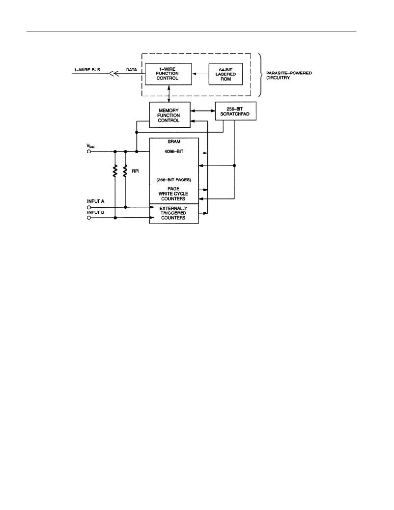
�DS2423�
�BLOCK� DIAGRAM� Figure� 1�
�ADDRESS� REGISTERS� AND� TRANSFER� STATUS�
�Because� of� the� serial� data� transfer,� the� DS2423� employs� three� address� registers� called� TA1,� TA2,� and� E/S�
�(Figure� 6).� Registers� TA1� and� TA2� must� be� loaded� with� the� target� address� to� which� the� data� will� be�
�written� or� from� which� data� will� be� sent� to� the� master� upon� a� Read� command.� Register� E/S� acts� like� a� byte�
�counter� and� Transfer� Status� register.� It� is� used� to� verify� data� integrity� with� write� commands.� Therefore,�
�the� master� only� has� read� access� to� this� register.� The� lower� 5� bits� of� the� E/S� register� indicate� the� address� of�
�the� last� byte� that� has� been� written� to� the� scratchpad.� This� address� is� called� Ending� Offset.� Bit� 5� of� the� E/S�
�register,� called� PF� or� “partial� byte� flag,”� is� set� if� the� number� of� data� bits� sent� by� the� master� is� not� an�
�integer� multiple� of� 8.� Bit� 6� has� no� function;� it� always� reads� 0.� Note� that� the� lowest� 5� bits� of� the� target�
�address� also� determine� the� address� within� the� scratchpad,� where� intermediate� storage� of� data� will� begin.�
�This� address� is� called� byte� offset.� If� the� target� address� (TA1)� for� a� Write� command� is� 03CH� for� example,�
�then� the� scratchpad� will� store� incoming� data� beginning� at� the� byte� offset� 1CH� and� will� be� full� after� only� 4�
�bytes.� The� corresponding� ending� offset� in� this� example� is� 1FH.� For� best� economy� of� speed� and� efficiency,�
�the� target� address� for� writing� should� point� to� the� beginning� of� a� new� page,� i.e.,� the� byte� offset� will� be� 0.�
�Thus� the� full� 32-byte� capacity� of� the� scratchpad� is� available,� resulting� also� in� the� ending� offset� of� 1FH.�
�However,� it� is� possible� to� write� one� or� several� contiguous� bytes� somewhere� within� a� page.� The� ending�
�offset� together� with� the� Partial� Flag� support� the� master� checking� the� data� integrity� after� a� Write� command.�
�The� highest� valued� bit� of� the� E/S� register,� called� AA� or� Authorization� Accepted,� acts� as� a� flag� to� indicate�
�that� the� data� stored� in� the� scratchpad� has� already� been� copied� to� the� target� memory� address.� Writing� data�
�to� the� scratchpad� clears� this� flag.�
�3� of� 25�
�相关PDF资料 |
PDF描述 |
|---|---|
| DS2430AP+T&R | IC EEPROM 256BIT 6TSOC |
| DS2431GA+U | IC EEPROM 1024BIT 2SFN |
| DS2433X-S#T | IC EEPROM 4KBIT 6FCHIP |
| DS2433X-Z01 | IC EEPROM 4KBIT 6FCHIP |
| DS24B33G+T&R | IC EEPROM 4KBIT 2SFN |
相关代理商/技术参数 |
参数描述 |
|---|---|
| DS2423MRAB0 | 制造商:Thomas & Betts 功能描述:300A,NLT,3P4W,MG,423,3P480V |
| DS2423P | 功能描述:静态随机存取存储器 RoHS:否 制造商:Cypress Semiconductor 存储容量:16 Mbit 组织:1 M x 16 访问时间:55 ns 电源电压-最大:3.6 V 电源电压-最小:2.2 V 最大工作电流:22 uA 最大工作温度:+ 85 C 最小工作温度:- 40 C 安装风格:SMD/SMT 封装 / 箱体:TSOP-48 封装:Tray |
| DS2423P/R | 制造商:DALLAS 制造商全称:Dallas Semiconductor 功能描述:4kbit 1-Wire RAM with Counter |
| DS2423P/T | 制造商:DALLAS 制造商全称:Dallas Semiconductor 功能描述:4kbit 1-Wire RAM with Counter |
| DS2423P/T&R | 功能描述:静态随机存取存储器 RoHS:否 制造商:Cypress Semiconductor 存储容量:16 Mbit 组织:1 M x 16 访问时间:55 ns 电源电压-最大:3.6 V 电源电压-最小:2.2 V 最大工作电流:22 uA 最大工作温度:+ 85 C 最小工作温度:- 40 C 安装风格:SMD/SMT 封装 / 箱体:TSOP-48 封装:Tray |
发布紧急采购,3分钟左右您将得到回复。