参数资料
| 型号: | DS26303DK |
| 厂商: | Maxim Integrated Products |
| 文件页数: | 13/43页 |
| 文件大小: | 0K |
| 描述: | KIT DESIGN FOR DS26303 |
| 产品培训模块: | Lead (SnPb) Finish for COTS Obsolescence Mitigation Program |
| 标准包装: | 1 |
| 主要目的: | 电信,线路接口单元(LIU) |
| 已用 IC / 零件: | DS26303 |
| 已供物品: | 板,线缆,电源 |
第1页第2页第3页第4页第5页第6页第7页第8页第9页第10页第11页第12页当前第13页第14页第15页第16页第17页第18页第19页第20页第21页第22页第23页第24页第25页第26页第27页第28页第29页第30页第31页第32页第33页第34页第35页第36页第37页第38页第39页第40页第41页第42页第43页
�� ���
���
���DS26303� Design� Kit�
�ID� REGISTERS�
�BID:� BOARD� ID� (Offset� =� 0X0000)�
�BID� is� read-only� with� a� value� of� 0xD.�
�XBIDH:� HIGH� NIBBLE� EXTENDED� BOARD� ID� (Offset� =� 0X0002)�
�XBIDH� is� read-only� with� a� value� of� 0x0.�
�XBIDM:� MIDDLE� NIBBLE� EXTENDED� BOARD� ID� (Offset� =� 0X0003)�
�XBIDM� is� read-only� with� a� value� of� 0x1.�
�XBIDL:� LOW� NIBBLE� EXTENDED� BOARD� ID� (Offset� =� 0X0004)�
�XBIDL� is� read-only� with� a� value� of� 0x6.�
�BREV:� BOARD� FAB� REVISION� (Offset� =� 0X0005)�
�BREV� is� read-only� and� displays� the� current� fab� revision.�
�AREV:� BOARD� ASSEMBLY� REVISION� (Offset� =� 0X0006)�
�AREV� is� read-only� and� displays� the� current� assembly� revision.�
�PREV:� FPGA� REVISION� (Offset� =� 0X0007)�
�PREV� is� read-only� and� displays� the� current� PLD� firmware� revision.�
�CONTROL� REGISTERS�
�Register� Name:� CTRL_1�
�Register� Description:� DS26303DK� FPGA� CONTROL� REGISTER� 1�
�Register� Offset:� 0x08�
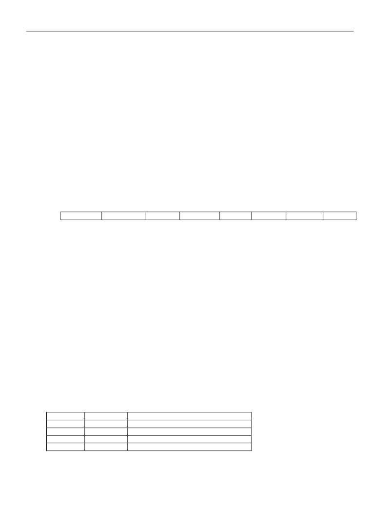
�Bit� #�
�Name�
�7�
�INT303�
�6�
�ENRLOS1�
�5�
�CLKE�
�4�
�SPI_SWAP�
�3�
�SPI�
�2�
�OE�
�1�
�MCLK1�
�0�
�MCLK0�
�Bit� 7:� INT303.� This� bit� indicates� the� status� of� the� INT303� line.�
�If� INT303� =� LOW,� there� is� no� hardware� interrupt� on� the� DS26303.�
�If� INT303� =� HIGH,� there� is� a� hardware� interrupt� on� the� DS26303.�
�Bit� 6:� ENRLOS1.� This� bit� enables� the� RLOS1� LED.� This� should� not� be� enabled� when� driving� TECLK� from� the�
�DS26303.�
�If� ENRLOS1� =� LOW,� the� RLOS1� LED� is� not� enabled.�
�If� ENRLOS1� =� HIGH,� the� RLOS1� LED� is� enabled� and� lights� when� RLOS1� is� high.�
�Bit� 5:� CLKE.� This� bit� sets� the� CLKE� pin� on� the� DS26303.� This� is� only� active� when� SPI� (Bit� 0)� is� HIGH.� If� SPI� (Bit� 0)�
�is� low,� CLKE� is� always� low.�
�If� CLKE� =� LOW,� SDO� is� clocked� out� on� the� rising� edge� of� SCLK.�
�If� CLKE� =� HIGH,� SDO� is� clocked� out� on� the� falling� edge� of� SCLK.�
�Bit� 4:� SPI_SWAP.� This� bit� sets� the� BSWP/A5� pin� on� the� DS26303.� This� is� only� active� when� SPI� (Bit� 0)� is� HIGH.�
�If� SPI_SWAP� =� LOW,� the� SPI� bus� is� LSB� first.�
�If� SPI_SWAP� =� HIGH,� the� SPI� bus� is� MSB� first.�
�Bit� 3:� SPI.� This� bit� sets� up� the� FPGA� to� use� serial� mode.� This� bit� also� changes� the� mode� pin� on� the� DS26303.�
�If� SPI� =� LOW,� the� parallel� bus� is� used� for� all� read/write� access.� This� also� sets� the� MODE� pin� on� the�
�DS26303� to� logic� 1.�
�If� SPI� =� HIGH,� the� SPI� bus� is� used� for� all� read/write� access.� This� also� sets� the� MODE� pin� on� the� DS26303�
�to� logic� 0.�
�Bit� 2:� OE.� This� bit� controls� the� OE� pin� to� the� DS26303.�
�Bits� 1� and� 0:� MCLK1� and� MCLK0.� These� bits� control� the� MCLK� pin� to� the� DS26303.�
�MCLK1�
�0�
�0�
�1�
�1�
�MCLK0�
�0�
�1�
�0�
�1�
�DESCRIPTION� OF� MCLK�
�MCLK� =� high-impedance� mode�
�MCLK� =� on-board� T1� oscillator�
�MCLK� =� on-board� E1� oscillator�
�MCLK� =� user� clock� input�
�13� of� 43�
�相关PDF资料 |
PDF描述 |
|---|---|
| DS26502DK | KIT DESIGN FOR DS26502 |
| DS26503DK | KIT DESIGN FOR DS26503 |
| DS26504DK | KIT DESIGN FOR DS26504 |
| DS26519DK | KIT DEMO FOR DS26519 |
| DS26521DK | KIT DESIGN FOR DS26521 |
相关代理商/技术参数 |
参数描述 |
|---|---|
| DS26303G-120 | 制造商:MAXIM 制造商全称:Maxim Integrated Products 功能描述:3.3V, E1/T1/J1, Short-Haul, Octal Line Interface Unit |
| DS26303G-75 | 制造商:MAXIM 制造商全称:Maxim Integrated Products 功能描述:3.3V, E1/T1/J1, Short-Haul, Octal Line Interface Unit |
| DS26303GN-120 | 制造商:MAXIM 制造商全称:Maxim Integrated Products 功能描述:3.3V, E1/T1/J1, Short-Haul, Octal Line Interface Unit |
| DS26303GN-75 | 制造商:MAXIM 制造商全称:Maxim Integrated Products 功能描述:3.3V, E1/T1/J1, Short-Haul, Octal Line Interface Unit |
| DS26303L-120 | 功能描述:电信线路管理 IC 3.3V E1/T1/J1 Short Haul Octal LIU RoHS:否 制造商:STMicroelectronics 产品:PHY 接口类型:UART 电源电压-最大:18 V 电源电压-最小:8 V 电源电流:30 mA 最大工作温度:+ 85 C 最小工作温度:- 40 C 安装风格:SMD/SMT 封装 / 箱体:VFQFPN-48 封装:Tray |
发布紧急采购,3分钟左右您将得到回复。