- 您现在的位置:买卖IC网 > PDF目录14304 > DS4510U-5+T&R (Maxim Integrated Products)IC SUPERVISOR W/NV MEM 10-USOP PDF资料下载
参数资料
| 型号: | DS4510U-5+T&R |
| 厂商: | Maxim Integrated Products |
| 文件页数: | 8/12页 |
| 文件大小: | 0K |
| 描述: | IC SUPERVISOR W/NV MEM 10-USOP |
| 产品培训模块: | Lead (SnPb) Finish for COTS Obsolescence Mitigation Program |
| 标准包装: | 3,000 |
| 类型: | 简单复位/加电复位 |
| 监视电压数目: | 1 |
| 输出: | 开路漏极或开路集电极 |
| 复位: | 低有效 |
| 复位超时: | 可调节/可选择 |
| 电压 - 阀值: | 4.625V |
| 工作温度: | -40°C ~ 85°C |
| 安装类型: | 表面贴装 |
| 封装/外壳: | 10-TFSOP,10-MSOP(0.118",3.00mm 宽) |
| 供应商设备封装: | 10-µMAX |
| 包装: | 带卷 (TR) |
�� �
�
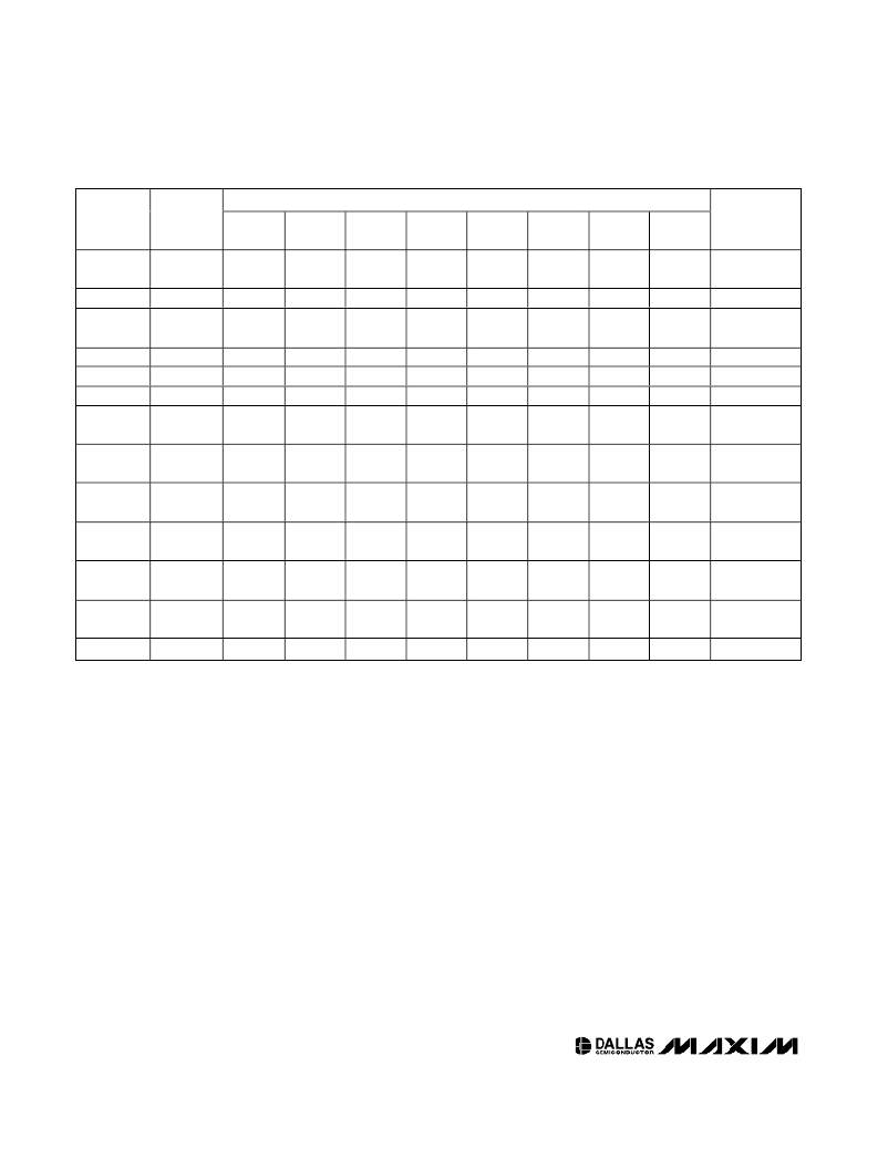
�CPU� Supervisor� with� Nonvolatile� Memory� and�
�Programmable� I/O�
�REGISTER�
�NAME�
�REGISTER�
�LOCATION�
�(HEX)�
�Bit� 7�
�Bit� 6�
�Bit5�
�REGISTER� BIT� NAMES�
�Bit� 4� Bit� 3�
�Bit� 2�
�Bit� 1�
�Bit� 0�
�FACTORY� OR�
�POWER-ON�
�DEFAULT�
�(BIN)�
�User�
�EEPROM�
�Reserved�
�Pullup�
�Enable�
�RST� Delay�
�User� SEE�
�User� SEE�
�I/O3�
�Control�
�I/O2�
�Control�
�I/O1�
�Control�
�I/O0�
�Control�
�I/O� Status�
�Config�
�User� SRAM�
�00-3F�
�40-EF�
�F0�
�F1�
�F2�
�F3�
�F4�
�F5�
�F6�
�F7�
�F8�
�F9�
�FA-FF�
�EE�
�n/a�
�SEE�
�SEE�
�SEE�
�SEE�
�SEE�
�SEE�
�SEE�
�SEE�
�0�
�ready�
�SRAM�
�EE�
�n/a�
�SEE�
�SEE�
�SEE�
�SEE�
�SEE�
�SEE�
�SEE�
�SEE�
�0�
�trip� point�
�SRAM�
�EE�
�n/a�
�SEE�
�SEE�
�SEE�
�SEE�
�SEE�
�SEE�
�SEE�
�SEE�
�0�
�reset�
�status�
�SRAM�
�EE�
�n/a�
�SEE�
�SEE�
�SEE�
�SEE�
�SEE�
�SEE�
�SEE�
�SEE�
�0�
�SEE�
�SRAM�
�EE�
�n/a�
�I/O3�
�pullup�
�SEE�
�SEE�
�SEE�
�SEE�
�SEE�
�SEE�
�SEE�
�I/O3�
�Status�
�SWRST�
�SRAM�
�EE�
�n/a�
�I/O2�
�pullup�
�SEE�
�SEE�
�SEE�
�SEE�
�SEE�
�SEE�
�SEE�
�I/O2�
�Status�
�0�
�SRAM�
�EE�
�n/a�
�I/O1�
�pullup�
�TD1�
�SEE�
�SEE�
�SEE�
�SEE�
�SEE�
�SEE�
�I/O1�
�Status�
�0�
�SRAM�
�EE�
�n/a�
�I/O0�
�pullup�
�TD0�
�SEE�
�SEE�
�I/O3�
�I/O2�
�I/O1�
�I/O0�
�I/O0�
�Status�
�0�
�SRAM�
�00000000�
�n/a�
�00000000�
�00000011�
�00000000�
�00000000�
�00000001�
�00000001�
�00000001�
�00000001�
�n/a�
�XXX00000�
�00000000�
�Figure� 4.� Register� Bit� Names�
�I� 2� C� Definitions�
�The� following� terminology� is� commonly� used� to�
�describe� I� 2� C� data� transfers.�
�Master� Device:� The� master� device� controls� the� slave�
�devices� on� the� bus.� The� master� device� generates� SCL�
�clock� pulses,� start,� and� stop� conditions.�
�Slave� Devices:� Slave� devices� send� and� receive� data�
�at� the� master’s� request.�
�Bus� Idle� or� Not� Busy:� Time� between� stop� and� start�
�conditions� when� both� SDA� and� SCL� are� inactive� and� in�
�their� logic-high� states.� When� the� bus� is� idle� it� often� initi-�
�ates� a� low-power� mode� for� slave� devices.�
�Start� Condition:� A� start� condition� is� generated� by� the�
�master� to� initiate� a� new� data� transfer� with� a� slave.�
�Transitioning� SDA� from� high� to� low� while� SCL� remains�
�high� generates� a� start� condition.� See� the� timing� dia-�
�gram� for� applicable� timing.�
�Stop� Condition:� A� stop� condition� is� generated� by� the�
�master� to� end� a� data� transfer� with� a� slave.� Transitioning�
�SDA� from� low� to� high� while� SCL� remains� high� gener-�
�ates� a� stop� condition.� See� the� I� 2� C� Timing� Diagram� for�
�applicable� timing.�
�Repeated� Start� Condition:� The� master� can� use� a�
�repeated� start� condition� at� the� end� of� one� data� transfer�
�to� indicate� that� it� will� immediately� initiate� a� new� data�
�transfer� following� the� current� one.� Repeated� starts� are�
�commonly� used� during� read� operations� to� identify� a�
�specific� memory� address� to� begin� a� data� transfer.� A�
�repeated� start� condition� is� issued� identically� to� a� nor-�
�mal� start� condition.� See� the� I� 2� C� Timing� Diagram� for�
�applicable� timing.�
�Bit� Write:� Transitions� of� SDA� must� occur� during� the� low�
�state� of� SCL.� The� data� on� SDA� must� remain� valid� and�
�unchanged� during� the� entire� high� pulse� of� SCL� (see�
�Figure� 5)� plus� the� setup� and� hold-time� requirements.�
�Data� is� shifted� into� the� device� during� the� rising� edge� of�
�the� SCL.�
�Bit� Read:� At� the� end� a� write� operation,� the� master� must�
�release� the� SDA� bus� line� for� the� proper� amount� of� setup�
�8�
�_____________________________________________________________________�
�相关PDF资料 |
PDF描述 |
|---|---|
| MAX6401BS24+T | IC SUPERVISOR MPU 4-UCSP |
| MAX6401BS25+T | IC SUPERVISOR MPU 4-UCSP |
| MAX6401BS28+T | IC SUPERVISOR MPU 4-UCSP |
| MAX6401BS27+T | IC SUPERVISOR MPU 4-UCSP |
| MAX6401BS26+T | IC SUPERVISOR MPU 4-UCSP |
相关代理商/技术参数 |
参数描述 |
|---|---|
| DS4514FP000 | 制造商:Thomas & Betts 功能描述:400A,CON,4P5W,MG,514,3PY347V |
| DS4514FP00K | 制造商:Thomas & Betts 功能描述:400AMP CON, 4P5W,MG,514,W/CONTACTS |
| DS4514FR000 | 制造商:Thomas & Betts 功能描述:400A,REC,4P5W,MG,514,3PY347V |
| DS4514FRAB0 | 制造商:Thomas & Betts 功能描述:400A,REC,4P5W,MG,514,3PY347V,AB0,SC |
| DS4514FRABK | 制造商:Thomas & Betts 功能描述:400A,REC,4P5W,MG,514,3P7347V,ABK,SC |
发布紧急采购,3分钟左右您将得到回复。