- 您现在的位置:买卖IC网 > PDF目录14304 > DS4510U-5+T&R (Maxim Integrated Products)IC SUPERVISOR W/NV MEM 10-USOP PDF资料下载
参数资料
| 型号: | DS4510U-5+T&R |
| 厂商: | Maxim Integrated Products |
| 文件页数: | 9/12页 |
| 文件大小: | 0K |
| 描述: | IC SUPERVISOR W/NV MEM 10-USOP |
| 产品培训模块: | Lead (SnPb) Finish for COTS Obsolescence Mitigation Program |
| 标准包装: | 3,000 |
| 类型: | 简单复位/加电复位 |
| 监视电压数目: | 1 |
| 输出: | 开路漏极或开路集电极 |
| 复位: | 低有效 |
| 复位超时: | 可调节/可选择 |
| 电压 - 阀值: | 4.625V |
| 工作温度: | -40°C ~ 85°C |
| 安装类型: | 表面贴装 |
| 封装/外壳: | 10-TFSOP,10-MSOP(0.118",3.00mm 宽) |
| 供应商设备封装: | 10-µMAX |
| 包装: | 带卷 (TR) |
�� �
�
�CPU� Supervisor� with� Nonvolatile� Memory� and�
�Programmable� I/O�
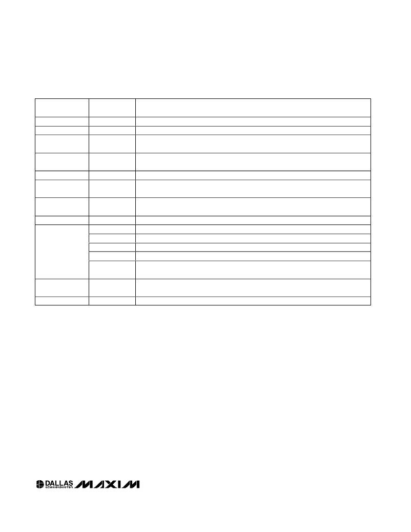
�Table� 1.� Register� Definitions�
�REGISTER�
�LOCATION� (HEX)�
�00� to� 3F�
�40� to� EF�
�F0�
�F1�
�F2� to� F3�
�F4� to� F7�
�F8�
�F9�
�FA� to� FF�
�REGISTER�
�NAME�
�User� EEPROM�
�Reserved�
�Pullup� Enable�
�RST� Delay�
�User� SEEPROM�
�I/O� X� Control�
�I/O� Status�
�Config�
�Bit� Name�
�ready�
�Trip� Point�
�Reset� Status�
�SEE�
�SWRST�
�User� SRAM�
�FUNCTION�
�64� bytes� of� EEPROM� memory.�
�These� memory� locations� are� reserved� for� future� products.�
�The� four� least� significant� bits� of� this� register� each� enable/disable� one� of� the� internal� pullup�
�resistors.� Set� the� bit� to� enable� the� pullup,� clear� it� to� disable� the� pullup.�
�The� two� LSBs� of� this� register� (TD1� and� TD0)� select� the� reset� delay� (t� RST� )� as� shown� in� the�
�CPU� Supervisor� AC� Timing� Characteristics� .�
�SRAM� Shadowed� EEPROM� user� byte.�
�Clearing� the� LSB� of� the� register� enables� the� I/O� X� pulldown� transistor;� setting� the� bit� disables�
�the� pulldown� transistor.�
�This� register� reflects� the� logic� level� of� the� I/O� X� pins.� The� upper� four� bits� of� this� register�
�always� read� zero.�
�This� register� contains� 5� bits� that� read� and� control� the� behavior� of� the� part� as� follows:�
�Bit� Function�
�Reads� zero� when� V� CC� is� above� the� DS4510's� power-on� reset� voltage.�
�Reads� one� when� V� CC� below� V� CCTP� .�
�Reads� one� when� the� RST� pin� is� active.�
�When� zero,� writes� to� the� SEEPROM� registers� behave� like� EEPROM.� When� one,� writes� to� the�
�SEEPROM� registers� behave� like� SRAM.�
�Setting� this� bit� activates� the� RST� output.� This� bit� automatically� returns� to� zero� during� the�
�RST� active� time.�
�6� bytes� of� SRAM� memory�
�time� (see� Figure� 5)� before� the� next� rising� edge� of� SCL�
�during� a� bit� read.� The� device� shifts� out� each� bit� of� data�
�on� SDA� at� the� falling� edge� of� the� previous� SCL� pulse�
�and� the� data� bit� is� valid� at� the� rising� edge� of� the� current�
�SCL� pulse.� Remember� that� the� master� generates� all�
�SCL� clock� pulses,� including� when� it� is� reading� bits� from�
�the� slave.�
�slave� to� the� master.� The� 8� bits� transmitted� by� the� mas-�
�ter� are� done� according� to� the� bit-write� definition� and� the�
�acknowledgement� is� read� using� the� bit-read� definition.�
�Byte� Read:� A� byte� read� is� an� 8-bit� information� transfer�
�from� the� slave� to� the� master� plus� a� 1-bit� ACK� or� NACK�
�from� the� master� to� the� slave.� The� 8� bits� of� information�
�that� are� transferred� (most� significant� bit� first)� from� the�
�Acknowledgement� (ACK� and� NACK):�
�An�
�slave� to� the� master� are� read� by� the� master� using� the�
�Acknowledgement� (ACK)� or� Not� Acknowledge� (NACK)�
�is� always� the� 9th� bit� transmitted� during� a� byte� transfer.�
�The� device� receiving� data� (the� master� during� a� read� or�
�the� slave� during� a� write� operation)� performs� an� ACK� by�
�transmitting� a� zero� during� the� 9th� bit.� A� device� per-�
�forms� a� NACK� by� transmitting� a� one� during� the� 9th� bit.�
�Timing� (� Figure� 5)� for� the� ACK� and� NACK� is� identical� to�
�all� other� bit� writes.� An� ACK� is� the� acknowledgment� that�
�the� device� is� properly� receiving� data.� A� NACK� is� used�
�to� terminate� a� read� sequence� or� as� an� indication� that�
�the� device� is� not� receiving� data.�
�Byte� Write:� A� byte� write� consists� of� 8� bits� of� informa-�
�tion� transferred� from� the� master� to� the� slave� (most� sig-�
�nificant� bit� first)� plus� a� 1-bit� acknowledgement� from� the�
�bit-read� definition� above,� and� the� master� transmits� an�
�ACK� using� the� bit-write� definition� to� receive� additional�
�data� bytes.� The� master� must� NACK� the� last� byte� read�
�to� terminate� communication� so� the� slave� will� return� con-�
�trol� of� SDA� to� the� master.�
�Slave� Address� and� the� R/� W� Bit:� Each� slave� on� the� I� 2� C�
�bus� responds� to� a� slave� addressing� byte� sent� immedi-�
�ately� following� a� start� condition.� The� slave� address� byte�
�contains� the� slave� address� and� the� R/� W� bit.� The� slave�
�address� (see� Figure� 6)� is� the� most� significant� 7� bits� and�
�the� R/� W� bit� is� the� least� significant� bit.�
�The� DS4510� ’s� slave� address� is� 101000A� 0� (binary),�
�where� A� 0� is� the� value� of� the� A� 0� address� pin.� The�
�_____________________________________________________________________�
�9�
�相关PDF资料 |
PDF描述 |
|---|---|
| MAX6401BS24+T | IC SUPERVISOR MPU 4-UCSP |
| MAX6401BS25+T | IC SUPERVISOR MPU 4-UCSP |
| MAX6401BS28+T | IC SUPERVISOR MPU 4-UCSP |
| MAX6401BS27+T | IC SUPERVISOR MPU 4-UCSP |
| MAX6401BS26+T | IC SUPERVISOR MPU 4-UCSP |
相关代理商/技术参数 |
参数描述 |
|---|---|
| DS4514FP000 | 制造商:Thomas & Betts 功能描述:400A,CON,4P5W,MG,514,3PY347V |
| DS4514FP00K | 制造商:Thomas & Betts 功能描述:400AMP CON, 4P5W,MG,514,W/CONTACTS |
| DS4514FR000 | 制造商:Thomas & Betts 功能描述:400A,REC,4P5W,MG,514,3PY347V |
| DS4514FRAB0 | 制造商:Thomas & Betts 功能描述:400A,REC,4P5W,MG,514,3PY347V,AB0,SC |
| DS4514FRABK | 制造商:Thomas & Betts 功能描述:400A,REC,4P5W,MG,514,3P7347V,ABK,SC |
发布紧急采购,3分钟左右您将得到回复。