- 您现在的位置:买卖IC网 > PDF目录97870 > DS83C530-QNL (MAXIM INTEGRATED PRODUCTS INC) 8-BIT, MROM, 33 MHz, MICROCONTROLLER, PQCC52 PDF资料下载
参数资料
| 型号: | DS83C530-QNL |
| 厂商: | MAXIM INTEGRATED PRODUCTS INC |
| 元件分类: | Microcontroller |
| 英文描述: | 8-BIT, MROM, 33 MHz, MICROCONTROLLER, PQCC52 |
| 封装: | PLASTIC, LCC-52 |
| 文件页数: | 28/45页 |
| 文件大小: | 649K |
| 代理商: | DS83C530-QNL |
第1页第2页第3页第4页第5页第6页第7页第8页第9页第10页第11页第12页第13页第14页第15页第16页第17页第18页第19页第20页第21页第22页第23页第24页第25页第26页第27页当前第28页第29页第30页第31页第32页第33页第34页第35页第36页第37页第38页第39页第40页第41页第42页第43页第44页第45页
DS87C530/DS83C530 EPROM/ROM Microcontrollers with Real-Time Clock
34 of 45
DC ELECTRICAL CHARACTERISTICS (continued)
(VCC = 4.5V to 5.5V, TA = -40°C to +85°C.)
PARAMETER
SYMBOL
MIN
TYP
MAX
UNITS
NOTES
Input Leakage Port 0,
EA, Pins, I/O Mode
IL
-10
+10
A
13
Input Leakage Port 0, Bus Mode
IL
-300
+300
A
14
RST Pulldown Resistance
RRST
50
200
k
Note 1:
Storage temperature is defined as the temperature of the device when VCC = 0V and VBAT = 0V. In this state, the contents of
SRAM are not battery backed and are undefined.
Note 2:
All parameters apply to both commercial and industrial temperature operation unless otherwise noted.
Note 3:
All voltages are referenced to ground.
Note 4:
Active current measured with 33MHz clock source on XTAL1, VCC = RST = 5.5V, other pins disconnected.
Note 5:
Idle mode current measured with 33MHz clock source on XTAL1, VCC = 5.5V, RST at ground, other pins disconnected.
Note 6:
Stop mode current measured with XTAL1 and RST grounded, VCC = 5.5V, all other pins disconnected.
Note 7:
VCC = 0V, VBAT = 3.3V. 32.768kHz crystal with 12.5pF load capacitance between RTCX1 and RTCX2 pins. RTCE bit set to 1.
Note 8:
RST = VCC. This condition mimics operation of pins in I/O mode. Port 0 is tri-stated in reset and when at a logic high state during
I/O mode.
Note 9:
During a 0-to-1 transition, a one-shot drives the ports hard for two clock cycles. This measurement reflects port in transition
mode.
Note 10:
When addressing external memory. This specification only applies to the first clock cycle following the transition.
Note 11:
This is the current required from an external circuit to hold a logic low level on an I/O pin while the corresponding port latch bit is
set to 1. This is only the current required to hold the low level; transitions from 1 to 0 on an I/O pin will also have to overcome the
transition current.
Note 12:
Ports 1, 2, and 3 source transition current when being pulled down externally. It reaches its maximum at approximately 2V.
Note 13:
0.45 < VIN < VCC. RST = VCC. This condition mimics operation of pins in I/O mode.
Note 14:
0.45 < VIN < VCC. Not a high-impedance input. This port is a weak address holding latch in Bus Mode. Peak current occurs near
the input transition point of the latch, approximately 2V.
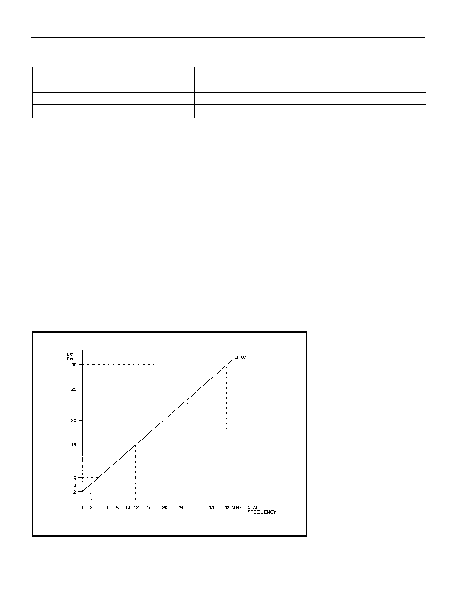
TYPICAL ICC vs. FREQUENCY
相关PDF资料 |
PDF描述 |
|---|---|
| DS87C530-QNL | 8-BIT, OTPROM, 33 MHz, MICROCONTROLLER, PQCC52 |
| DS83C530-QCL | 8-BIT, MROM, 33 MHz, MICROCONTROLLER, PQCC52 |
| DS87C530-KCL | 8-BIT, OTPROM, 33 MHz, MICROCONTROLLER, CQCC52 |
| DTA-03D-1.5-TA-P | POSITION, LINEAR SENSOR-AC, -3-3mm |
| DTA-01D-3-SA-P | POSITION, LINEAR SENSOR-AC, -1-1mm |
相关代理商/技术参数 |
参数描述 |
|---|---|
| DS83C530-QNL+ | 制造商:DALLAS 制造商全称:Dallas Semiconductor 功能描述:EPROM/ROM Microcontrollers with Real-Time Clock |
| DS83CH20 | 制造商:未知厂家 制造商全称:未知厂家 功能描述:Peripheral (Multifunction) Controller |
| DS84 | 制造商:未知厂家 制造商全称:未知厂家 功能描述:Analog IC |
| DS840 | 制造商:未知厂家 制造商全称:未知厂家 功能描述:Analog IC |
| DS843 | 制造商:未知厂家 制造商全称:未知厂家 功能描述:Analog IC |
发布紧急采购,3分钟左右您将得到回复。