- 您现在的位置:买卖IC网 > PDF目录1917 > DSP56311VF150B1 (Freescale Semiconductor)IC DSP 24BIT 150MHZ 196-BGA PDF资料下载
参数资料
| 型号: | DSP56311VF150B1 |
| 厂商: | Freescale Semiconductor |
| 文件页数: | 45/96页 |
| 文件大小: | 0K |
| 描述: | IC DSP 24BIT 150MHZ 196-BGA |
| 标准包装: | 630 |
| 系列: | DSP56K/Symphony |
| 类型: | 定点 |
| 接口: | 主机接口,SSI,SCI |
| 时钟速率: | 150MHz |
| 非易失内存: | ROM(576 B) |
| 芯片上RAM: | 384kB |
| 电压 - 输入/输出: | 3.30V |
| 电压 - 核心: | 1.80V |
| 工作温度: | -40°C ~ 100°C |
| 安装类型: | 表面贴装 |
| 封装/外壳: | 196-LBGA |
| 供应商设备封装: | 196-MAPBGA(15x15) |
| 包装: | 托盘 |
第1页第2页第3页第4页第5页第6页第7页第8页第9页第10页第11页第12页第13页第14页第15页第16页第17页第18页第19页第20页第21页第22页第23页第24页第25页第26页第27页第28页第29页第30页第31页第32页第33页第34页第35页第36页第37页第38页第39页第40页第41页第42页第43页第44页当前第45页第46页第47页第48页第49页第50页第51页第52页第53页第54页第55页第56页第57页第58页第59页第60页第61页第62页第63页第64页第65页第66页第67页第68页第69页第70页第71页第72页第73页第74页第75页第76页第77页第78页第79页第80页第81页第82页第83页第84页第85页第86页第87页第88页第89页第90页第91页第92页第93页第94页第95页第96页
DSP56311 Technical Data, Rev. 8
Freescale Semiconductor
1-1
Signals/Connections
1
The DSP56311 input and output signals are organized into functional groups as shown in Table 1-1. Figure 1-1
diagrams the DSP56311 signals by functional group. The remainder of this chapter describes the signal pins in
each functional group.
Note:
The Clock Output (CLKOUT), BCLK, BCLK, CAS, and RAS[0–3] signals used by other DSP56300 family members
are supported by the DSP56311 at operating frequencies up to 100 MHz. Therefore, above 100 MHz, you must
enable bus arbitration by setting the Asynchronous Bus Arbitration Enable Bit (ABE) in the operating mode register.
When set, the ABE bit eliminates the required set-up and hold times for BB and BG with respect to CLKOUT. In
addition, DRAM access is not supported above 100 MHz.
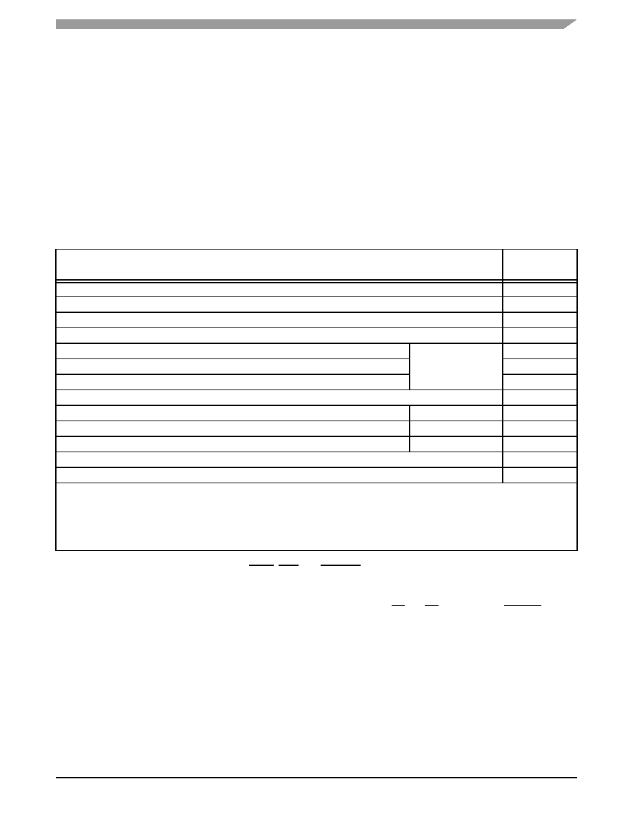
Table 1-1.
DSP56311 Functional Signal Groupings
Functional Group
Number of
Signals
Power (VCC)
20
Ground (GND)
66
Clock
2
PLL
3
Address bus
Port A
1
18
Data bus
24
Bus control
13
Interrupt and mode control
5
Host interface (HI08)
Port B2
16
Enhanced synchronous serial interface (ESSI)
Ports C and D
3
12
Serial communication interface (SCI)
Port E4
3
Timer
3
OnCE/JTAG Port
6
Notes:
1.
Port A signals define the external memory interface port, including the external address bus, data bus, and control signals.
2.
Port B signals are the HI08 port signals multiplexed with the GPIO signals.
3.
Port C and D signals are the two ESSI port signals multiplexed with the GPIO signals.
4.
Port E signals are the SCI port signals multiplexed with the GPIO signals.
5.
There are 5 signal connections that are not used. These are designated as no connect (NC) in the package description (see
相关PDF资料 |
PDF描述 |
|---|---|
| DSP56321VF200R2 | IC DSP 24BIT 200MHZ 196-BGA |
| DSP56852VFE | IC DSP 16BIT 120MHZ 81-MAPBGA |
| DSP56854FGE | IC DSP 16BIT 120MHZ 128-LQFP |
| DSP56855BUE | IC DSP 16BIT 120MHZ 100-LQFP |
| DSP56857BUE | IC DSP 16BIT 120MHZ 100-LQFP |
相关代理商/技术参数 |
参数描述 |
|---|---|
| DSP56311VF150R2 | 功能描述:数字信号处理器和控制器 - DSP, DSC 24 BIT DSP RoHS:否 制造商:Microchip Technology 核心:dsPIC 数据总线宽度:16 bit 程序存储器大小:16 KB 数据 RAM 大小:2 KB 最大时钟频率:40 MHz 可编程输入/输出端数量:35 定时器数量:3 设备每秒兆指令数:50 MIPs 工作电源电压:3.3 V 最大工作温度:+ 85 C 封装 / 箱体:TQFP-44 安装风格:SMD/SMT |
| DSP56311VF160 | 功能描述:数字信号处理器和控制器 - DSP, DSC SSP26111VF160A RoHS:否 制造商:Microchip Technology 核心:dsPIC 数据总线宽度:16 bit 程序存储器大小:16 KB 数据 RAM 大小:2 KB 最大时钟频率:40 MHz 可编程输入/输出端数量:35 定时器数量:3 设备每秒兆指令数:50 MIPs 工作电源电压:3.3 V 最大工作温度:+ 85 C 封装 / 箱体:TQFP-44 安装风格:SMD/SMT |
| DSP56311VL150 | 功能描述:数字信号处理器和控制器 - DSP, DSC 24 BIT DSP PBFREE RoHS:否 制造商:Microchip Technology 核心:dsPIC 数据总线宽度:16 bit 程序存储器大小:16 KB 数据 RAM 大小:2 KB 最大时钟频率:40 MHz 可编程输入/输出端数量:35 定时器数量:3 设备每秒兆指令数:50 MIPs 工作电源电压:3.3 V 最大工作温度:+ 85 C 封装 / 箱体:TQFP-44 安装风格:SMD/SMT |
| DSP56311VL150B1 | 功能描述:数字信号处理器和控制器 - DSP, DSC 24 BIT DSP PBFREE RoHS:否 制造商:Microchip Technology 核心:dsPIC 数据总线宽度:16 bit 程序存储器大小:16 KB 数据 RAM 大小:2 KB 最大时钟频率:40 MHz 可编程输入/输出端数量:35 定时器数量:3 设备每秒兆指令数:50 MIPs 工作电源电压:3.3 V 最大工作温度:+ 85 C 封装 / 箱体:TQFP-44 安装风格:SMD/SMT |
| DSP56311VL150R2 | 功能描述:数字信号处理器和控制器 - DSP, DSC 24 BIT DSP PBFREE RoHS:否 制造商:Microchip Technology 核心:dsPIC 数据总线宽度:16 bit 程序存储器大小:16 KB 数据 RAM 大小:2 KB 最大时钟频率:40 MHz 可编程输入/输出端数量:35 定时器数量:3 设备每秒兆指令数:50 MIPs 工作电源电压:3.3 V 最大工作温度:+ 85 C 封装 / 箱体:TQFP-44 安装风格:SMD/SMT |
发布紧急采购,3分钟左右您将得到回复。