- 您现在的位置:买卖IC网 > PDF目录1917 > DSP56311VF150B1 (Freescale Semiconductor)IC DSP 24BIT 150MHZ 196-BGA PDF资料下载
参数资料
| 型号: | DSP56311VF150B1 |
| 厂商: | Freescale Semiconductor |
| 文件页数: | 78/96页 |
| 文件大小: | 0K |
| 描述: | IC DSP 24BIT 150MHZ 196-BGA |
| 标准包装: | 630 |
| 系列: | DSP56K/Symphony |
| 类型: | 定点 |
| 接口: | 主机接口,SSI,SCI |
| 时钟速率: | 150MHz |
| 非易失内存: | ROM(576 B) |
| 芯片上RAM: | 384kB |
| 电压 - 输入/输出: | 3.30V |
| 电压 - 核心: | 1.80V |
| 工作温度: | -40°C ~ 100°C |
| 安装类型: | 表面贴装 |
| 封装/外壳: | 196-LBGA |
| 供应商设备封装: | 196-MAPBGA(15x15) |
| 包装: | 托盘 |
第1页第2页第3页第4页第5页第6页第7页第8页第9页第10页第11页第12页第13页第14页第15页第16页第17页第18页第19页第20页第21页第22页第23页第24页第25页第26页第27页第28页第29页第30页第31页第32页第33页第34页第35页第36页第37页第38页第39页第40页第41页第42页第43页第44页第45页第46页第47页第48页第49页第50页第51页第52页第53页第54页第55页第56页第57页第58页第59页第60页第61页第62页第63页第64页第65页第66页第67页第68页第69页第70页第71页第72页第73页第74页第75页第76页第77页当前第78页第79页第80页第81页第82页第83页第84页第85页第86页第87页第88页第89页第90页第91页第92页第93页第94页第95页第96页
DSP56311 Technical Data, Rev. 8
1-4
Freescale Semiconductor
Signals/Connections
1.4 PLL
1.5 External Memory Expansion Port (Port A)
Note:
When the DSP56311 enters a low-power standby mode (stop or wait), it releases bus mastership and tri-
states the relevant Port A signals: A[0–17], D[0–23], AA[0–3], RD, WR, BB.
1.5.1
External Address Bus
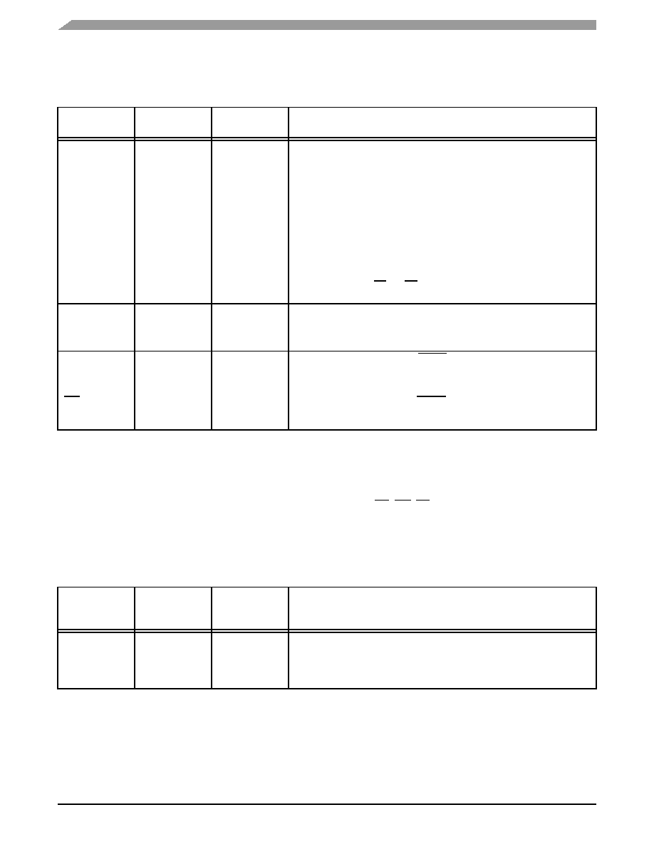
Table 1-5.
Phase-Locked Loop Signals
Signal Name
Type
State During
Reset
Signal Description
CLKOUT
Output
Chip-driven
Clock Output—Provides an output clock synchronized to the internal core
clock phase.
If the PLL is enabled and both the multiplication and division factors equal one,
then CLKOUT is also synchronized to EXTAL.
If the PLL is disabled, the CLKOUT frequency is half the frequency of EXTAL.
Note: At operating frequencies above 100 MHz, this signal produces a low-
amplitude waveform that is not usable externally by other devices. Above 100
MHz, you can use the asynchronous bus arbitration option that is enabled by
the Asynchronous Bus Arbitration Enable (ABE) bit in the Operating Mode
Register. When set, the DSP enters the Asynchronous Arbitration mode,
which eliminates the BB and BG set-up and hold time requirements with
respect to CLKOUT.
PCAP
Input
PLL Capacitor—An input connecting an off-chip capacitor to the PLL filter.
Connect one capacitor terminal to PCAP and the other terminal to VCCP.
If the PLL is not used, PCAP can be tied to VCC, GND, or left floating.
PINIT
NMI
Input
PLL Initial—During assertion of RESET, the value of PINIT is written into the
PLL enable (PEN) bit of the PLL control (PCTL) register, determining whether
the PLL is enabled or disabled.
Nonmaskable Interrupt—After RESET deassertion and during normal
instruction processing, this Schmitt-trigger input is the negative-edge-triggered
NMI request internally synchronized to CLKOUT.
Table 1-6.
External Address Bus Signals
Signal Name
Type
State During
Reset, Stop,
or Wait
Signal Description
A[0–17]
Output
Tri-stated
Address Bus—When the DSP is the bus master, A[0–17] are active-high
outputs that specify the address for external program and data memory
accesses. Otherwise, the signals are tri-stated. To minimize power dissipation,
A[0–17] do not change state when external memory spaces are not being
accessed.
相关PDF资料 |
PDF描述 |
|---|---|
| DSP56321VF200R2 | IC DSP 24BIT 200MHZ 196-BGA |
| DSP56852VFE | IC DSP 16BIT 120MHZ 81-MAPBGA |
| DSP56854FGE | IC DSP 16BIT 120MHZ 128-LQFP |
| DSP56855BUE | IC DSP 16BIT 120MHZ 100-LQFP |
| DSP56857BUE | IC DSP 16BIT 120MHZ 100-LQFP |
相关代理商/技术参数 |
参数描述 |
|---|---|
| DSP56311VF150R2 | 功能描述:数字信号处理器和控制器 - DSP, DSC 24 BIT DSP RoHS:否 制造商:Microchip Technology 核心:dsPIC 数据总线宽度:16 bit 程序存储器大小:16 KB 数据 RAM 大小:2 KB 最大时钟频率:40 MHz 可编程输入/输出端数量:35 定时器数量:3 设备每秒兆指令数:50 MIPs 工作电源电压:3.3 V 最大工作温度:+ 85 C 封装 / 箱体:TQFP-44 安装风格:SMD/SMT |
| DSP56311VF160 | 功能描述:数字信号处理器和控制器 - DSP, DSC SSP26111VF160A RoHS:否 制造商:Microchip Technology 核心:dsPIC 数据总线宽度:16 bit 程序存储器大小:16 KB 数据 RAM 大小:2 KB 最大时钟频率:40 MHz 可编程输入/输出端数量:35 定时器数量:3 设备每秒兆指令数:50 MIPs 工作电源电压:3.3 V 最大工作温度:+ 85 C 封装 / 箱体:TQFP-44 安装风格:SMD/SMT |
| DSP56311VL150 | 功能描述:数字信号处理器和控制器 - DSP, DSC 24 BIT DSP PBFREE RoHS:否 制造商:Microchip Technology 核心:dsPIC 数据总线宽度:16 bit 程序存储器大小:16 KB 数据 RAM 大小:2 KB 最大时钟频率:40 MHz 可编程输入/输出端数量:35 定时器数量:3 设备每秒兆指令数:50 MIPs 工作电源电压:3.3 V 最大工作温度:+ 85 C 封装 / 箱体:TQFP-44 安装风格:SMD/SMT |
| DSP56311VL150B1 | 功能描述:数字信号处理器和控制器 - DSP, DSC 24 BIT DSP PBFREE RoHS:否 制造商:Microchip Technology 核心:dsPIC 数据总线宽度:16 bit 程序存储器大小:16 KB 数据 RAM 大小:2 KB 最大时钟频率:40 MHz 可编程输入/输出端数量:35 定时器数量:3 设备每秒兆指令数:50 MIPs 工作电源电压:3.3 V 最大工作温度:+ 85 C 封装 / 箱体:TQFP-44 安装风格:SMD/SMT |
| DSP56311VL150R2 | 功能描述:数字信号处理器和控制器 - DSP, DSC 24 BIT DSP PBFREE RoHS:否 制造商:Microchip Technology 核心:dsPIC 数据总线宽度:16 bit 程序存储器大小:16 KB 数据 RAM 大小:2 KB 最大时钟频率:40 MHz 可编程输入/输出端数量:35 定时器数量:3 设备每秒兆指令数:50 MIPs 工作电源电压:3.3 V 最大工作温度:+ 85 C 封装 / 箱体:TQFP-44 安装风格:SMD/SMT |
发布紧急采购,3分钟左右您将得到回复。