- 您现在的位置:买卖IC网 > PDF目录10940 > DSP56F807VF80 (Freescale Semiconductor)IC DSP 80MHZ 60K FLASH 160-BGA PDF资料下载
参数资料
| 型号: | DSP56F807VF80 |
| 厂商: | Freescale Semiconductor |
| 文件页数: | 13/60页 |
| 文件大小: | 0K |
| 描述: | IC DSP 80MHZ 60K FLASH 160-BGA |
| 标准包装: | 126 |
| 系列: | 56F8xx |
| 核心处理器: | 56800 |
| 芯体尺寸: | 16-位 |
| 速度: | 80MHz |
| 连通性: | CAN,EBI/EMI,SCI,SPI |
| 外围设备: | POR,PWM,WDT |
| 输入/输出数: | 32 |
| 程序存储器容量: | 136KB(68K x 16) |
| 程序存储器类型: | 闪存 |
| RAM 容量: | 6K x 16 |
| 电压 - 电源 (Vcc/Vdd): | 3 V ~ 3.6 V |
| 数据转换器: | A/D 16x12b |
| 振荡器型: | 外部 |
| 工作温度: | -40°C ~ 85°C |
| 封装/外壳: | 160-BGA |
| 包装: | 托盘 |
第1页第2页第3页第4页第5页第6页第7页第8页第9页第10页第11页第12页当前第13页第14页第15页第16页第17页第18页第19页第20页第21页第22页第23页第24页第25页第26页第27页第28页第29页第30页第31页第32页第33页第34页第35页第36页第37页第38页第39页第40页第41页第42页第43页第44页第45页第46页第47页第48页第49页第50页第51页第52页第53页第54页第55页第56页第57页第58页第59页第60页
56F807 Technical Data Technical Data, Rev. 16
20
Freescale Semiconductor
2.14 JTAG/OnCE
Part 3 Specifications
3.1 General Characteristics
The 56F807 is fabricated in high-density CMOS with 5V-tolerant TTL-compatible digital inputs. The term
“5V-tolerant” refers to the capability of an I/O pin, built on a 3.3V compatible process technology, to
withstand a voltage up to 5.5V without damaging the device. Many systems have a mixture of devices
designed for 3.3V and 5V power supplies. In such systems, a bus may carry both 3.3V and 5V-compatible
I/O voltage levels (a standard 3.3V I/O is designed to receive a maximum voltage of 3.3V
± 10% during
normal operation without causing damage). This 5V-tolerant capability therefore offers the power savings
of 3.3V I/O levels while being able to receive 5V levels without being damaged.
Absolute maximum ratings given in Table 3-1 are stress ratings only, and functional operation at the
maximum is not guaranteed. Stress beyond these ratings may affect device reliability or cause permanent
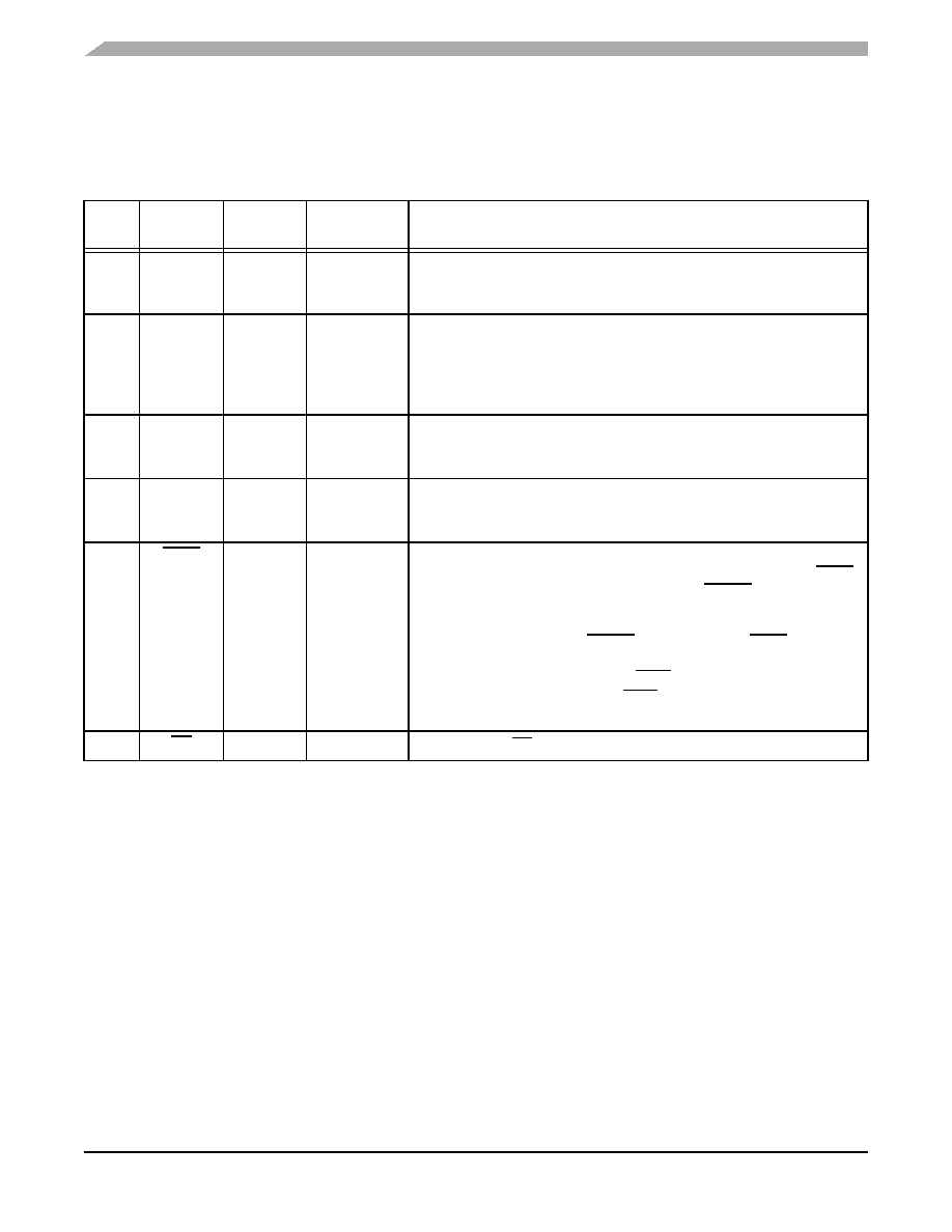
Table 2-19 JTAG/On-Chip Emulation (OnCE) Signals
No. of
Pins
Signal
Name
Signal
Type
State During
Reset
Signal Description
1
TCK
Input
(Schmitt)
Input, pulled
low internally
Test Clock Input—This input pin provides a gated clock to synchronize
the test logic and shift serial data to the JTAG/OnCE port. The pin is
connected internally to a pull-down resistor.
1
TMS
Input
(Schmitt)
Input, pulled
high internally
Test Mode Select Input—This input pin is used to sequence the JTAG
TAP controller’s state machine. It is sampled on the rising edge of TCK
and has an on-chip pull-up resistor.
Note:
Always tie the TMS pin to VDD through a 2.2K resistor.
1
TDI
Input
(Schmitt)
Input, pulled
high internally
Test Data Input—This input pin provides a serial input data stream to
the JTAG/OnCE port. It is sampled on the rising edge of TCK and has an
on-chip pull-up resistor.
1
TDO
Output
Tri-stated
Test Data Output—This tri-statable output pin provides a serial output
data stream from the JTAG/OnCE port. It is driven in the Shift-IR and
Shift-DR controller states, and changes on the falling edge of TCK.
1
TRST
Input
(Schmitt)
Input, pulled
high internally
Test Reset—As an input, a low signal on this pin provides a reset signal
to the JTAG TAP controller. To ensure complete hardware reset, TRST
should be asserted at power-up and whenever RESET is asserted. The
only exception occurs in a debugging environment when a hardware
device reset is required and it is necessary not to reset the OnCE/JTAG
module. In this case, assert RESET, but do not assert TRST.
Note:
For normal operation, connect TRST directly to VSS. If the design is to
be used in a debugging environment, TRST may be tied to VSS through a 1K
resistor.
1
DE
Output
Debug Event—DE provides a low pulse on recognized debug events.
相关PDF资料 |
PDF描述 |
|---|---|
| VI-B20-IW-B1 | CONVERTER MOD DC/DC 5V 100W |
| MC9328MXLCVM15 | IC MCU I.MXL 150MHZ 256-MAPBGA |
| VI-2NX-CU-S | CONVERTER MOD DC/DC 5.2V 200W |
| CS42L51-CNZR | IC CODEC LOW-V 24BIT 32-QFP |
| VI-2NW-CU-S | CONVERTER MOD DC/DC 5.5V 200W |
相关代理商/技术参数 |
参数描述 |
|---|---|
| DSP56F807VF80E | 功能描述:数字信号处理器和控制器 - DSP, DSC 16 BIT HYBRID CONTROLLER RoHS:否 制造商:Microchip Technology 核心:dsPIC 数据总线宽度:16 bit 程序存储器大小:16 KB 数据 RAM 大小:2 KB 最大时钟频率:40 MHz 可编程输入/输出端数量:35 定时器数量:3 设备每秒兆指令数:50 MIPs 工作电源电压:3.3 V 最大工作温度:+ 85 C 封装 / 箱体:TQFP-44 安装风格:SMD/SMT |
| DSP56F807VF80E | 制造商:Freescale Semiconductor 功能描述:Digital Signal Processor IC |
| DSP56F807VF80J | 制造商:Freescale Semiconductor 功能描述:DSP 16BIT - Trays |
| DSP56F826 | 制造商:FREESCALE 制造商全称:Freescale Semiconductor, Inc 功能描述:16-bit Digital Signal Controllers |
| DSP56F826-827UM | 制造商:未知厂家 制造商全称:未知厂家 功能描述:16-Bit Digital Signal Processor Users Manual |
发布紧急采购,3分钟左右您将得到回复。