- 您现在的位置:买卖IC网 > Datasheet目录323 > DSPAUDIOEVMMB1E (Freescale Semiconductor)BOARD MOTHER DSP563XX Datasheet资料下载
参数资料
| 型号: | DSPAUDIOEVMMB1E |
| 厂商: | Freescale Semiconductor |
| 文件页数: | 11/60页 |
| 文件大小: | 0K |
| 描述: | BOARD MOTHER DSP563XX |
| 标准包装: | 1 |
| 系列: | Symphony™ |
| 类型: | DSP |
| 适用于相关产品: | DSP563XX |
| 所含物品: | 主板 |
第1页第2页第3页第4页第5页第6页第7页第8页第9页第10页当前第11页第12页第13页第14页第15页第16页第17页第18页第19页第20页第21页第22页第23页第24页第25页第26页第27页第28页第29页第30页第31页第32页第33页第34页第35页第36页第37页第38页第39页第40页第41页第42页第43页第44页第45页第46页第47页第48页第49页第50页第51页第52页第53页第54页第55页第56页第57页第58页第59页第60页
�� �
�
�Signal� Headers�
�2.2.4.5�
�JP10� –� Config� /� Debug� MPU� Communication�
�The� JP10� jumpers� provide� a� communication� port� between� the� debug� microcontroller� and� the� configuration� microcontroller.� When� the� SDI�
�debugger� is� used� and� the� AUX5� jumper� is� out,� the� SDI� debugger� interface� controls� the� audio� input� source.� The� JP10� jumpers� provide� a�
�communication� port� between� the� debug� microcontroller� and� the� configuration� microcontroller.� When� the� SDI� debugger� is� used,� and� the� AUX5�
�jumper� is� out,� the� SDI� debugger� interface� controls� the� audio� input� source.� To� allow� this,� all� JP10� jumpers� should� be� populated.�
�2.2.4.6�
�JP11� –� AUX� Mode� Input� Source� Selection�
�The� JP11� jumpers� are� present� as� an� alternative� to� using� the� SDI� debugger� software� to� select� between� the� various� inputs� available.� If� the� AUX5�
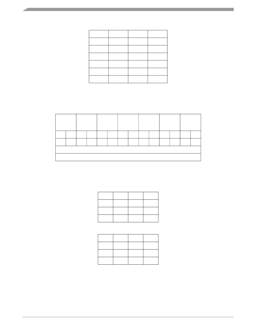
�jumper� is� present� then� the� following� jumper� settings� will� result� in� the� input� selection� shown� in� Table� 2-5�
�Table� 2-5.� JP11� Selections�
�Input� Selected�
�RX1�
�RX2�
�RX3�
�RX4�
�AIN1�
�SDI�
�Aux5�
�1�
�1�
�1�
�1�
�1�
�0�
�Aux4*�
�0�
�0�
�0�
�0�
�0�
�X�
�Aux3�
�0�
�0�
�0�
�0�
�1�
�X�
�Aux2�
�0�
�0�
�1�
�1�
�0�
�X�
�Aux1�
�0�
�1�
�0�
�1�
�0�
�X�
�debugger�
�selects� input�
�*� When� the� Aux5� jumper� is� present,� the� Aux4� jumper� directly�
�controls� the� mute� functionality� of� the� EVM� motherboard.�
�2.3�
�Signal� Headers�
�These� headers� allow� for� external� debugger� connections,� analog� output� signal� measurement,� and� GPIO� access.�
�2.3.1�
�P1� —� PPI� Header�
�The� PPI� header� connections� are� to� allow� for� backwards� compatibility� with� existing� PPI� software� tool� set� and� to� allow� easy� access� to� the� SHI�
�port� connections� from� the� motherboard.� Note� that� when� using� PPI� source,� JP8� must� have� PPI� Port� jumper� in� place.�
�Table� 2-6.� P1� —� PPI� Header�
�2.3.2�
�NC(1)�
�GND�
�GND�
�SDA�
�VDD�
�P2� —� OnCE� Header�
�*�
�*�
�*�
�*�
�*�
�*�
�*�
�*�
�*�
�*�
�SS/HA2�
�SCK/SCL�
�HREQ�
�MOSI� /� HA0�
�MISO�
�The� P2� OnCE� header� is� for� connection� of� an� external� OnCE/JTAG� debugger� tool� to� the� OnCE/JTAG� port� of� the� DSP� on� the� daughterboard.�
�Further� explanation� of� the� OnCE/JTAG� signal� definition� can� be� found� in� the� DSP� users� guides.� The� P2� OnCE� header� is� for� connection� of� an�
�external� OnCE/JTAG� debugger� tool� to� the� OnCE/JTAG� port� of� the� DSP� on� the� daughterboard.� Further� explanation� of� the� OnCE/JTAG� signal�
�definition� can� be� found� in� the� DSP� users� guides.� Note� that� when� using� an� external� OnCE/JTAG� debugger� tool,� the� JP9� JTAG� jumper� should�
�be� in� the� "OnCE"� position.�
�DSPAUDIOEVM� Users� Guide,� Rev.� 2.4�
�This� document� contains� information� on� a� new� product.� Specifications� and� information� herein� are� subject� ot� change� without� notice.�
�Freescale� Semiconductor�
�5�
�相关PDF资料 |
PDF描述 |
|---|---|
| DSPIC30F2010 DEVELOPMENT KIT | KIT DEV EMBEDDED C |
| DSTRM-KT-0181A | DSTREAM DEBUG AND TRACE UNIT |
| DSUT1CSU | SURGE SUPPR NETWORK W/GROUND |
| DTEL2 | SURGE SUPPRESSOR PHONE RJ11/RJ45 |
| DV003001 | PROGRAMMER PICSTART PLUS 16C/17C |
相关代理商/技术参数 |
参数描述 |
|---|---|
| DSPB362DB1 | 功能描述:子卡和OEM板 B VERSION 362 DAUGHTER C RoHS:否 制造商:BeagleBoard by CircuitCo 产品:BeagleBone LCD4 Boards 用于:BeagleBone - BB-Bone - Open Source Development Kit |
| DSPB364DB1 | 功能描述:子卡和OEM板 B VERSION 364 DAUGHTER C RoHS:否 制造商:BeagleBoard by CircuitCo 产品:BeagleBone LCD4 Boards 用于:BeagleBone - BB-Bone - Open Source Development Kit |
| DSPB366DB1 | 功能描述:子卡和OEM板 B VERSION 366 DAUGHTER C RoHS:否 制造商:BeagleBoard by CircuitCo 产品:BeagleBone LCD4 Boards 用于:BeagleBone - BB-Bone - Open Source Development Kit |
| DSPB367DB1 | 功能描述:子卡和OEM板 B VERSION 367 DAUGHTER C RoHS:否 制造商:BeagleBoard by CircuitCo 产品:BeagleBone LCD4 Boards 用于:BeagleBone - BB-Bone - Open Source Development Kit |
| DSPB371DB1 | 功能描述:DAUGHTER CARD B 56371 RoHS:是 类别:编程器,开发系统 >> 过时/停产零件编号 系列:- 标准包装:1 系列:- 传感器类型:CMOS 成像,彩色(RGB) 传感范围:WVGA 接口:I²C 灵敏度:60 fps 电源电压:5.7 V ~ 6.3 V 嵌入式:否 已供物品:成像器板 已用 IC / 零件:KAC-00401 相关产品:4H2099-ND - SENSOR IMAGE WVGA COLOR 48-PQFP4H2094-ND - SENSOR IMAGE WVGA MONO 48-PQFP |
发布紧急采购,3分钟左右您将得到回复。