- 您现在的位置:买卖IC网 > PDF目录11486 > DSPIC30F2011-20I/P (Microchip Technology)IC DSPIC MCU/DSP 12K 18DIP PDF资料下载
参数资料
| 型号: | DSPIC30F2011-20I/P |
| 厂商: | Microchip Technology |
| 文件页数: | 12/66页 |
| 文件大小: | 0K |
| 描述: | IC DSPIC MCU/DSP 12K 18DIP |
| 产品培训模块: | Serial Communications using dsPIC30F I2C Serial Communications using dsPIC30F SPI Serial Communications using dsPIC30F UART dsPIC30F 12 bit ADC - Part 2 dsPIC30F Addressing Modes - Part 1 dsPIC30F Architecture - Part 1 dsPIC30F DSP Engine & ALU dsPIC30F Interrupts dsPIC30F Motor Control PWM dsPIC Timers Asynchronous Stimulus dsPIC30F Addressing Modes - Part 2 dsPIC30F Architecture - Part 2 dsPIC30F 12-bit ADC Part 1 |
| 标准包装: | 25 |
| 系列: | dsPIC™ 30F |
| 核心处理器: | dsPIC |
| 芯体尺寸: | 16-位 |
| 速度: | 20 MIPS |
| 连通性: | I²C,SPI,UART/USART |
| 外围设备: | 欠压检测/复位,POR,PWM,WDT |
| 输入/输出数: | 12 |
| 程序存储器容量: | 12KB(4K x 24) |
| 程序存储器类型: | 闪存 |
| RAM 容量: | 1K x 8 |
| 电压 - 电源 (Vcc/Vdd): | 2.5 V ~ 5.5 V |
| 数据转换器: | A/D 8x12b |
| 振荡器型: | 内部 |
| 工作温度: | -40°C ~ 85°C |
| 封装/外壳: | 18-DIP(0.300",7.62mm) |
| 包装: | 管件 |
| 配用: | AC30F005-ND - MODULE SCKT DSPIC30F 18DIP/SOIC ACICE0202-ND - ADAPTER MPLABICE 18P 300 MIL |
| 其它名称: | DSPIC30F2011-20IP |
第1页第2页第3页第4页第5页第6页第7页第8页第9页第10页第11页当前第12页第13页第14页第15页第16页第17页第18页第19页第20页第21页第22页第23页第24页第25页第26页第27页第28页第29页第30页第31页第32页第33页第34页第35页第36页第37页第38页第39页第40页第41页第42页第43页第44页第45页第46页第47页第48页第49页第50页第51页第52页第53页第54页第55页第56页第57页第58页第59页第60页第61页第62页第63页第64页第65页第66页
dsPIC30F Flash Programming Specification
DS70102K-page 2
2010 Microchip Technology Inc.
2.2
Pins Used During Programming
The pins identified in Table 2-1 are used for device
programming. Refer to the appropriate device data
sheet for complete pin descriptions.
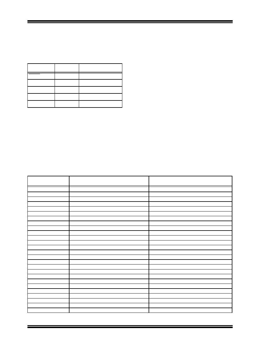
TABLE 2-1:
dsPIC30F PIN DESCRIPTIONS
DURING PROGRAMMING
Pin Name
Pin Type
Pin Description
MCLR/VPP
P
Programming Enable
VDD
P
Power Supply
VSS
P
Ground
PGC
I
Serial Clock
PGD
I/O
Serial Data
2.3
Program Memory Map
The program memory space extends from 0x0 to
0xFFFFFE. Code storage is located at the base of the
memory map and supports up to 144 Kbytes (48K
instruction words). Code is stored in three, 48 Kbyte
memory panels that reside on-chip. Table 2-2 shows
the location and program memory size of each device.
Locations 0x800000 through 0x8005BE are reserved
for executive code memory. This region stores either
the programming executive or debugging executive.
The programming executive is used for device
programming, while the debug executive is used for in-
circuit debugging. This region of memory cannot be
used to store user code.
Locations 0xF80000 through 0xF8000E are reserved
for the Configuration registers. The bits in these
registers may be set to select various device options,
and are described in Section 5.7 “Configuration Bits
Locations 0xFF0000 and 0xFF0002 are reserved for
the Device ID registers. These bits can be used by the
programmer to identify what device type is being
programmed and are described in Section 10.0
“Device ID”. The device ID reads out normally, even
after code protection is applied.
Figure 2-2 illustrates the memory map for the
dsPIC30F devices.
2.4
Data EEPROM Memory
The Data EEPROM array supports up to 4 Kbytes of
data and is located in one memory panel. It is mapped
in program memory space, residing at the end of User
Memory Space (see Figure 2-2). Table 2-2 shows the
location and size of data EEPROM in each device.
TABLE 2-2:
CODE MEMORY AND DATA EEPROM MAP AND SIZE
Device
Code Memory map
(Size in Instruction Words)
Data EEPROM Memory Map
(Size in Bytes)
dsPIC30F2010
0x000000-0x001FFE (4K)
0x7FFC00-0x7FFFFE (1K)
dsPIC30F2011
0x000000-0x001FFE (4K)
None (0K)
dsPIC30F2012
0x000000-0x001FFE (4K)
None (0K)
dsPIC30F3010
0x000000-0x003FFE (8K)
0x7FFC00-0x7FFFFE (1K)
dsPIC30F3011
0x000000-0x003FFE (8K)
0x7FFC00-0x7FFFFE (1K)
dsPIC30F3012
0x000000-0x003FFE (8K)
0x7FFC00-0x7FFFFE (1K)
dsPIC30F3013
0x000000-0x003FFE (8K)
0x7FFC00-0x7FFFFE (1K)
dsPIC30F3014
0x000000-0x003FFE (8K)
0x7FFC00-0x7FFFFE (1K)
dsPIC30F4011
0x000000-0x007FFE (16K)
0x7FFC00-0x7FFFFE (1K)
dsPIC30F4012
0x000000-0x007FFE (16K)
0x7FFC00-0x7FFFFE (1K)
dsPIC30F4013
0x000000-0x007FFE (16K)
0x7FFC00-0x7FFFFE (1K)
dsPIC30F5011
0x000000-0x00AFFE (22K)
0x7FFC00-0x7FFFFE (1K)
dsPIC30F5013
0x000000-0x00AFFE (22K)
0x7FFC00-0x7FFFFE (1K)
dsPIC30F5015
0x000000-0x00AFFE (22K)
0x7FFC00-0x7FFFFE (1K)
dsPIC30F5016
0x000000-0x00AFFE (22K)
0x7FFC00-0x7FFFFE (1K)
dsPIC30F6010
0x000000-0x017FFE (48K)
0x7FF000-0x7FFFFE (4K)
dsPIC30F6010A
0x000000-0x017FFE (48K)
0x7FF000-0x7FFFFF (4K)
dsPIC30F6011
0x000000-0x015FFE (44K)
0x7FF800-0x7FFFFE (2K)
dsPIC30F6011A
0x000000-0x015FFE (44K)
0x7FF800-0x7FFFFE (2K)
dsPIC30F6012
0x000000-0x017FFE (48K)
0x7FF000-0x7FFFFE (4K)
dsPIC30F6012A
0x000000-0x017FFE (48K)
0x7FF000-0x7FFFFE (4K)
dsPIC30F6013
0x000000-0x015FFE (44K)
0x7FF800-0x7FFFFE (2K)
dsPIC30F6013A
0x000000-0x015FFE (44K)
0x7FF800-0x7FFFFE (2K)
dsPIC30F6014
0x000000-0x017FFE (48K)
0x7FF000-0x7FFFFE (4K)
dsPIC30F6014A
0x000000-0x017FFE (48K)
0x7FF000-0x7FFFFE (4K)
dsPIC30F6015
0x000000-0x017FFE (48K)
0x7FF000-0x7FFFFE (4K)
Legend: I = Input, O = Output, P = Power
相关PDF资料 |
PDF描述 |
|---|---|
| ADV3220ACPZ | IC MULTIPLEXER 2:1 16LFCSP |
| GRM319F51E105ZA01D | CAP CER 1UF 25V Y5V 1206 |
| ADV3219ACPZ | IC MULTIPLEXER 2:1 16LFCSP |
| GRM2197U2A4R7CD01D | CAP CER 4.7PF 100V U2J 0805 |
| ADG636YRUZ | IC SWITCH DUAL SPDT 14TSSOP |
相关代理商/技术参数 |
参数描述 |
|---|---|
| dsPIC30F2011-30I/ML | 功能描述:数字信号处理器和控制器 - DSP, DSC 28LD 30MIPS 12 KB RoHS:否 制造商:Microchip Technology 核心:dsPIC 数据总线宽度:16 bit 程序存储器大小:16 KB 数据 RAM 大小:2 KB 最大时钟频率:40 MHz 可编程输入/输出端数量:35 定时器数量:3 设备每秒兆指令数:50 MIPs 工作电源电压:3.3 V 最大工作温度:+ 85 C 封装 / 箱体:TQFP-44 安装风格:SMD/SMT |
| dsPIC30F2011-30I/P | 功能描述:数字信号处理器和控制器 - DSP, DSC 18LD 30MIPS 12 KB RoHS:否 制造商:Microchip Technology 核心:dsPIC 数据总线宽度:16 bit 程序存储器大小:16 KB 数据 RAM 大小:2 KB 最大时钟频率:40 MHz 可编程输入/输出端数量:35 定时器数量:3 设备每秒兆指令数:50 MIPs 工作电源电压:3.3 V 最大工作温度:+ 85 C 封装 / 箱体:TQFP-44 安装风格:SMD/SMT |
| DSPIC30F2011-30I/P | 制造商:Microchip Technology Inc 功能描述:16- Bit Digital Signal Controller |
| dsPIC30F2011-30I/SO | 功能描述:数字信号处理器和控制器 - DSP, DSC 18LD 30MIPS 12 KB RoHS:否 制造商:Microchip Technology 核心:dsPIC 数据总线宽度:16 bit 程序存储器大小:16 KB 数据 RAM 大小:2 KB 最大时钟频率:40 MHz 可编程输入/输出端数量:35 定时器数量:3 设备每秒兆指令数:50 MIPs 工作电源电压:3.3 V 最大工作温度:+ 85 C 封装 / 箱体:TQFP-44 安装风格:SMD/SMT |
| DSPIC30F2011-30I/SO | 制造商:Microchip Technology Inc 功能描述:16- Bit Digital Signal Controller |
发布紧急采购,3分钟左右您将得到回复。