- 您现在的位置:买卖IC网 > PDF目录11393 > DSPIC30F2020T-30I/SO (Microchip Technology)IC DSPIC MCU/DSP 12K 28SOIC PDF资料下载
参数资料
| 型号: | DSPIC30F2020T-30I/SO |
| 厂商: | Microchip Technology |
| 文件页数: | 31/285页 |
| 文件大小: | 0K |
| 描述: | IC DSPIC MCU/DSP 12K 28SOIC |
| 产品培训模块: | Asynchronous Stimulus |
| 标准包装: | 1 |
| 系列: | dsPIC™ 30F |
| 核心处理器: | dsPIC |
| 芯体尺寸: | 16-位 |
| 速度: | 30 MIP |
| 连通性: | I²C,IrDA,LIN,SPI,UART/USART |
| 外围设备: | 欠压检测/复位,POR,PWM,WDT |
| 输入/输出数: | 21 |
| 程序存储器容量: | 12KB(4K x 24) |
| 程序存储器类型: | 闪存 |
| RAM 容量: | 512 x 8 |
| 电压 - 电源 (Vcc/Vdd): | 3 V ~ 5.5 V |
| 数据转换器: | A/D 8x10b |
| 振荡器型: | 内部 |
| 工作温度: | -40°C ~ 85°C |
| 封装/外壳: | 28-SOIC(0.295",7.50mm 宽) |
| 包装: | 标准包装 |
| 配用: | DM300023-ND - KIT DEMO DSPICDEM SMPS BUCK DV164005-ND - KIT ICD2 SIMPLE SUIT W/USB CABLE |
| 其它名称: | DSPIC30F2020T-30I/SODKR |
第1页第2页第3页第4页第5页第6页第7页第8页第9页第10页第11页第12页第13页第14页第15页第16页第17页第18页第19页第20页第21页第22页第23页第24页第25页第26页第27页第28页第29页第30页当前第31页第32页第33页第34页第35页第36页第37页第38页第39页第40页第41页第42页第43页第44页第45页第46页第47页第48页第49页第50页第51页第52页第53页第54页第55页第56页第57页第58页第59页第60页第61页第62页第63页第64页第65页第66页第67页第68页第69页第70页第71页第72页第73页第74页第75页第76页第77页第78页第79页第80页第81页第82页第83页第84页第85页第86页第87页第88页第89页第90页第91页第92页第93页第94页第95页第96页第97页第98页第99页第100页第101页第102页第103页第104页第105页第106页第107页第108页第109页第110页第111页第112页第113页第114页第115页第116页第117页第118页第119页第120页第121页第122页第123页第124页第125页第126页第127页第128页第129页第130页第131页第132页第133页第134页第135页第136页第137页第138页第139页第140页第141页第142页第143页第144页第145页第146页第147页第148页第149页第150页第151页第152页第153页第154页第155页第156页第157页第158页第159页第160页第161页第162页第163页第164页第165页第166页第167页第168页第169页第170页第171页第172页第173页第174页第175页第176页第177页第178页第179页第180页第181页第182页第183页第184页第185页第186页第187页第188页第189页第190页第191页第192页第193页第194页第195页第196页第197页第198页第199页第200页第201页第202页第203页第204页第205页第206页第207页第208页第209页第210页第211页第212页第213页第214页第215页第216页第217页第218页第219页第220页第221页第222页第223页第224页第225页第226页第227页第228页第229页第230页第231页第232页第233页第234页第235页第236页第237页第238页第239页第240页第241页第242页第243页第244页第245页第246页第247页第248页第249页第250页第251页第252页第253页第254页第255页第256页第257页第258页第259页第260页第261页第262页第263页第264页第265页第266页第267页第268页第269页第270页第271页第272页第273页第274页第275页第276页第277页第278页第279页第280页第281页第282页第283页第284页第285页
dsPIC30F1010/202X
DS70178C-page 124
Preliminary
2006 Microchip Technology Inc.
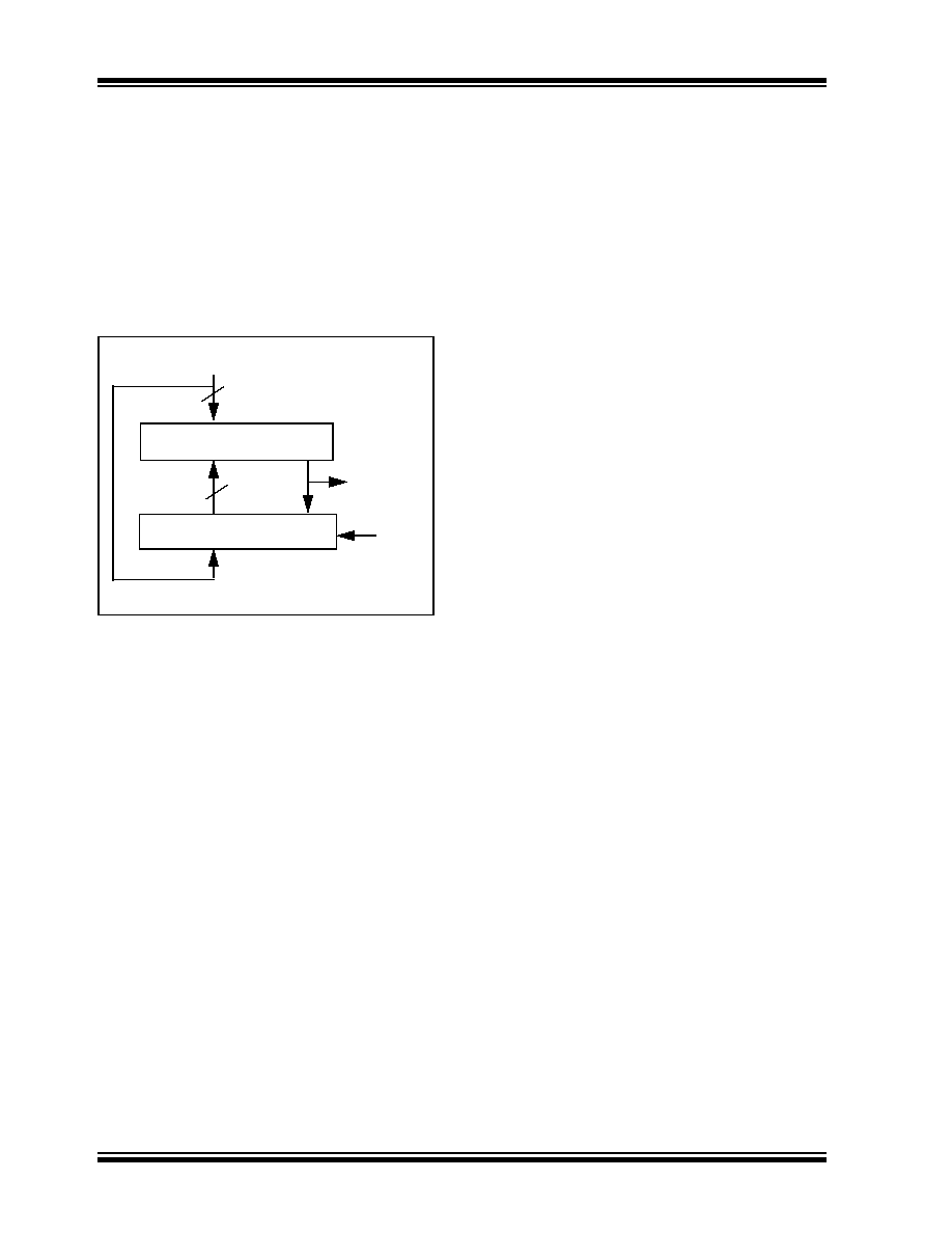
12.5
Primary PWM Time Base
There is a Primary Time Base (PTMR) counter for the
entire PWM module, In addition, each PWM generator
has an individual time base counter.
The PTMR determines when the individual time base
counters are to update their duty cycle and phase-shift
registers. The master time base is also responsible for
generating the Special Event Triggers and timer-based
interrupts. Figure 12-12 shows a block diagram of the
primary time base logic.
FIGURE 12-12:
PTMR BLOCK DIAGRAM
The primary time base may be reset by an external
signal specified via the SYNCSRC<2:0> bits in the
PTCON register. The external reset feature is enabled
via the SYNCEN bit in the PTCON register. The pri-
mary time base reset feature supports synchronization
of the primary time base with another SMPS dsPIC
DSC device or other circuitry in the user’s application.
The primary time base logic also provides an output
signal when a period match occurs that can be used to
synchronize an external device such as another
SMPS dsPIC DSC.
12.5.1
PTMR SYNCHRONIZATION
Because absolute synchronization is not possible, the
user should program the time base period of the sec-
ondary (slave) device to be slightly larger than the pri-
mary device time base to ensure that the two time
bases will reset at the same time.
12.6
Primary PWM Time Base Roll
Counter
The primary time base has an additional 6-bit counter
that counts the period matches of the primary time
base. This ROLL counter enables the PWM genera-
tors to stagger their trigger events in time to the ADC
module. This counter is not accessible for reading.
Each PWM generator has six bits (TRGSTRT<5:0>) in
the TRGCONx registers. These bits are used to spec-
ify the start enable for each TRIGx postscaler con-
trolled by the TRGDIV<2:0> bits in the TRGCONx
registers.
The TRGDIV bits specify how frequently a trigger
pulse is generated, and the ROLL bits specify when
the sequence begins. Once the TRIG postscaler is
enabled, the ROLL bits and the TRGSTRT bits have
no further effect until the PWM module is disabled and
then reenabled.
The purpose of the ROLL counter and the TRGSTRT
bits is to allow the user to spread the system work load
over a series of PWM cycles.
An additional use of the ROLL counter is to allow the
internal FRC oscillator to be varied on a PWM cycle
basis to reduce peak EMI emissions generated by
switching transistors in the power conversion
application.
The ROLL counter is cleared when the PWM module
is disabled (PTEN = 0), and the TRIGx postscalers are
disabled, requiring a new ROLL versus TRGSTRT
match to begin counting again.
12.7
Individual PWM Time Base(s)
Each PWM generator also has its own PWM time
base. Figure 12-13 shows a block diagram for the indi-
vidual time base circuits. With a time base per PWM
generator, the PWM module can generate PWM out-
puts that are phase shifted relative to each other, or
totally independent of each other. The individual PWM
timers (TMRx) provide the time base values that are
compared to the duty cycle registers to create the
PWM signals. The user may initialize these individual
time base counters before or during operation via the
phase-shift registers. The primary (PTMR) and the
individual timers (TMRx) are not user readable.
PTMR
PERIOD
Equality Comparator
Clk
>
Reset
13
PR_MATCH
相关PDF资料 |
PDF描述 |
|---|---|
| VE-B64-IY | CONVERTER MOD DC/DC 48V 50W |
| VE-B61-IY | CONVERTER MOD DC/DC 12V 50W |
| VE-26R-IY | CONVERTER MOD DC/DC 7.5V 50W |
| VE-26M-IY | CONVERTER MOD DC/DC 10V 50W |
| VE-B60-IY | CONVERTER MOD DC/DC 5V 50W |
相关代理商/技术参数 |
参数描述 |
|---|---|
| dsPIC30F2023-20E/ML | 功能描述:数字信号处理器和控制器 - DSP, DSC 12KB 512bytes-RAM 30MIPS 35I/O RoHS:否 制造商:Microchip Technology 核心:dsPIC 数据总线宽度:16 bit 程序存储器大小:16 KB 数据 RAM 大小:2 KB 最大时钟频率:40 MHz 可编程输入/输出端数量:35 定时器数量:3 设备每秒兆指令数:50 MIPs 工作电源电压:3.3 V 最大工作温度:+ 85 C 封装 / 箱体:TQFP-44 安装风格:SMD/SMT |
| dsPIC30F2023-20E/PT | 功能描述:数字信号处理器和控制器 - DSP, DSC 12KB 512bytes RAM 30MIPS 35I/O RoHS:否 制造商:Microchip Technology 核心:dsPIC 数据总线宽度:16 bit 程序存储器大小:16 KB 数据 RAM 大小:2 KB 最大时钟频率:40 MHz 可编程输入/输出端数量:35 定时器数量:3 设备每秒兆指令数:50 MIPs 工作电源电压:3.3 V 最大工作温度:+ 85 C 封装 / 箱体:TQFP-44 安装风格:SMD/SMT |
| dsPIC30F2023-30I/ML | 功能描述:数字信号处理器和控制器 - DSP, DSC 12KB 512bytes-RAM 30MIPS 35I/O RoHS:否 制造商:Microchip Technology 核心:dsPIC 数据总线宽度:16 bit 程序存储器大小:16 KB 数据 RAM 大小:2 KB 最大时钟频率:40 MHz 可编程输入/输出端数量:35 定时器数量:3 设备每秒兆指令数:50 MIPs 工作电源电压:3.3 V 最大工作温度:+ 85 C 封装 / 箱体:TQFP-44 安装风格:SMD/SMT |
| dsPIC30F2023-30I/PT | 功能描述:数字信号处理器和控制器 - DSP, DSC 12KB 512bytes-RAM 30MIPS 35I/O RoHS:否 制造商:Microchip Technology 核心:dsPIC 数据总线宽度:16 bit 程序存储器大小:16 KB 数据 RAM 大小:2 KB 最大时钟频率:40 MHz 可编程输入/输出端数量:35 定时器数量:3 设备每秒兆指令数:50 MIPs 工作电源电压:3.3 V 最大工作温度:+ 85 C 封装 / 箱体:TQFP-44 安装风格:SMD/SMT |
| DSPIC30F2023-30I/PTD32 | 功能描述:IC DSPIC MCU/DSP 12K 44-TQFP RoHS:是 类别:集成电路 (IC) >> 嵌入式 - 微控制器, 系列:dsPIC™ 30F 产品培训模块:The Ultra-Low Power MSP430 MSP430 Overview MSP430 Design Tools MSP430 Peripherals MSP430 for Utility Metering Solutions MSP430: How to JTAG MSP430, How To Use the Clock System Grace Software Graphical User Interface MCU Overview Driver Library MSP430Ware Overview 标准包装:60 系列:MSP430F2xx 核心处理器:RISC 芯体尺寸:16-位 速度:12MHz 连通性:SPI,UART/USART 外围设备:欠压检测/复位,PWM,WDT 输入/输出数:11 程序存储器容量:4KB(4K x 8) 程序存储器类型:闪存 EEPROM 大小:- RAM 容量:256 x 8 电压 - 电源 (Vcc/Vdd):1.8 V ~ 3.6 V 数据转换器:A/D 3x24b 振荡器型:内部 工作温度:-40°C ~ 85°C 封装/外壳:24-TSSOP(0.173",4.40mm 宽) 包装:管件 |
发布紧急采购,3分钟左右您将得到回复。