- 您现在的位置:买卖IC网 > PDF目录11356 > DSPIC30F3012-20I/P (Microchip Technology)IC DSPIC MCU/DSP 24K 18DIP PDF资料下载
参数资料
| 型号: | DSPIC30F3012-20I/P |
| 厂商: | Microchip Technology |
| 文件页数: | 111/161页 |
| 文件大小: | 0K |
| 描述: | IC DSPIC MCU/DSP 24K 18DIP |
| 产品培训模块: | Serial Communications using dsPIC30F I2C Serial Communications using dsPIC30F SPI Serial Communications using dsPIC30F UART dsPIC30F 12 bit ADC - Part 2 dsPIC30F Addressing Modes - Part 1 dsPIC30F Architecture - Part 1 dsPIC30F DSP Engine & ALU dsPIC30F Interrupts dsPIC30F Motor Control PWM dsPIC Timers Asynchronous Stimulus dsPIC30F Addressing Modes - Part 2 dsPIC30F Architecture - Part 2 dsPIC30F 12-bit ADC Part 1 |
| 标准包装: | 25 |
| 系列: | dsPIC™ 30F |
| 核心处理器: | dsPIC |
| 芯体尺寸: | 16-位 |
| 速度: | 20 MIPS |
| 连通性: | I²C,SPI,UART/USART |
| 外围设备: | 欠压检测/复位,POR,PWM,WDT |
| 输入/输出数: | 12 |
| 程序存储器容量: | 24KB(8K x 24) |
| 程序存储器类型: | 闪存 |
| EEPROM 大小: | 1K x 8 |
| RAM 容量: | 2K x 8 |
| 电压 - 电源 (Vcc/Vdd): | 2.5 V ~ 5.5 V |
| 数据转换器: | A/D 8x12b |
| 振荡器型: | 内部 |
| 工作温度: | -40°C ~ 85°C |
| 封装/外壳: | 18-DIP(0.300",7.62mm) |
| 包装: | 管件 |
| 配用: | AC30F005-ND - MODULE SCKT DSPIC30F 18DIP/SOIC ACICE0202-ND - ADAPTER MPLABICE 18P 300 MIL |
| 其它名称: | DSPIC30F3012-20IP |
第1页第2页第3页第4页第5页第6页第7页第8页第9页第10页第11页第12页第13页第14页第15页第16页第17页第18页第19页第20页第21页第22页第23页第24页第25页第26页第27页第28页第29页第30页第31页第32页第33页第34页第35页第36页第37页第38页第39页第40页第41页第42页第43页第44页第45页第46页第47页第48页第49页第50页第51页第52页第53页第54页第55页第56页第57页第58页第59页第60页第61页第62页第63页第64页第65页第66页第67页第68页第69页第70页第71页第72页第73页第74页第75页第76页第77页第78页第79页第80页第81页第82页第83页第84页第85页第86页第87页第88页第89页第90页第91页第92页第93页第94页第95页第96页第97页第98页第99页第100页第101页第102页第103页第104页第105页第106页第107页第108页第109页第110页当前第111页第112页第113页第114页第115页第116页第117页第118页第119页第120页第121页第122页第123页第124页第125页第126页第127页第128页第129页第130页第131页第132页第133页第134页第135页第136页第137页第138页第139页第140页第141页第142页第143页第144页第145页第146页第147页第148页第149页第150页第151页第152页第153页第154页第155页第156页第157页第158页第159页第160页第161页
2010 Microchip Technology Inc.
DS70139G-page 39
dsPIC30F2011/2012/3012/3013
All byte loads into any W register are loaded into the
LSB. The MSB is not modified.
A Sign-Extend (SE) instruction is provided to allow
users to translate 8-bit signed data to 16-bit signed
values. Alternatively, for 16-bit unsigned data, users
can clear the MSB of any W register by executing a
Zero-Extend (ZE) instruction on the appropriate
address.
Although most instructions are capable of operating on
word or byte data sizes, it should be noted that some
instructions, including the DSP instructions, operate
only on words.
3.2.5
NEAR DATA SPACE
An 8 Kbyte near data space is reserved in X address
memory space between 0x0000 and 0x1FFF, which is
directly addressable via a 13-bit absolute address field
within all memory direct instructions. The remaining X
address space and all of the Y address space is
addressable indirectly. Additionally, the whole of X data
space is addressable using MOV instructions, which
support memory direct addressing with a 16-bit
address field.
3.2.6
SOFTWARE STACK
The dsPIC DSC devices contain a software stack. W15
is used as the Stack Pointer.
The Stack Pointer always points to the first available
free word and grows from lower addresses towards
higher addresses. It pre-decrements for stack pops
and post-increments for stack pushes, as shown in
Figure 3-10. Note that for a PC push during any CALL
instruction, the MSB of the PC is zero-extended before
the push, ensuring that the MSB is always clear.
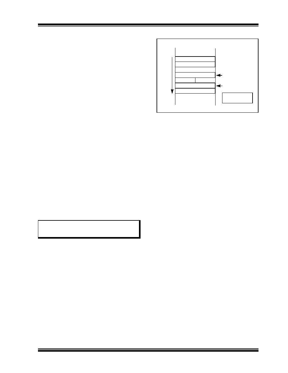
FIGURE 3-10:
CALL
STACK FRAME
There is a Stack Pointer Limit register (SPLIM)
associated
with
the
Stack
Pointer.
SPLIM
is
uninitialized at Reset. As is the case for the Stack
Pointer, SPLIM<0> is forced to ‘0’ because all stack
operations must be word aligned. Whenever an
Effective Address (EA) is generated using W15 as a
source or destination pointer, the address thus
generated is compared with the value in SPLIM. If the
contents of the Stack Pointer (W15) and the SPLIM reg-
ister are equal, and a push operation is performed, a
stack error trap does not occur. The stack error trap
occurs on a subsequent push operation. Thus, for
example, if it is desirable to cause a stack error trap
when the stack grows beyond address 0x2000 in RAM,
initialize the SPLIM with the value, 0x1FFE.
Similarly, a Stack Pointer underflow (stack error) trap is
generated when the Stack Pointer address is found to
be less than 0x0800, thus preventing the stack from
interfering with the Special Function Register (SFR)
space.
A write to the SPLIM register should not be immediately
followed by an indirect read operation using W15.
Note:
A PC push during exception processing
concatenates the SRL register to the MSB
of the PC prior to the push.
<Free Word>
PC<15:0>
000000000
0
15
W15 (before CALL)
W15 (after CALL)
S
tac
k
Gr
ow
s
T
o
w
a
rd
s
Hi
gh
er
A
d
re
s
0x0000
PC<22:16>
POP
: [--W15]
PUSH : [W15++]
相关PDF资料 |
PDF描述 |
|---|---|
| V375A32E600BL | CONVERTER MOD DC/DC 32V 600W |
| V375A32E600B3 | CONVERTER MOD DC/DC 32V 600W |
| V375A32E600B | CONVERTER MOD DC/DC 32V 600W |
| VE-B2Y-IY-S | CONVERTER MOD DC/DC 3.3V 33W |
| VE-B2Y-IX-S | CONVERTER MOD DC/DC 3.3V 49.5W |
相关代理商/技术参数 |
参数描述 |
|---|---|
| DSPIC30F3012-30I/ML | 功能描述:数字信号处理器和控制器 - DSP, DSC Sensor RoHS:否 制造商:Microchip Technology 核心:dsPIC 数据总线宽度:16 bit 程序存储器大小:16 KB 数据 RAM 大小:2 KB 最大时钟频率:40 MHz 可编程输入/输出端数量:35 定时器数量:3 设备每秒兆指令数:50 MIPs 工作电源电压:3.3 V 最大工作温度:+ 85 C 封装 / 箱体:TQFP-44 安装风格:SMD/SMT |
| DSPIC30F3012-30I/P | 功能描述:数字信号处理器和控制器 - DSP, DSC Sensor RoHS:否 制造商:Microchip Technology 核心:dsPIC 数据总线宽度:16 bit 程序存储器大小:16 KB 数据 RAM 大小:2 KB 最大时钟频率:40 MHz 可编程输入/输出端数量:35 定时器数量:3 设备每秒兆指令数:50 MIPs 工作电源电压:3.3 V 最大工作温度:+ 85 C 封装 / 箱体:TQFP-44 安装风格:SMD/SMT |
| DSPIC30F3012-30I/SO | 功能描述:数字信号处理器和控制器 - DSP, DSC Sensor RoHS:否 制造商:Microchip Technology 核心:dsPIC 数据总线宽度:16 bit 程序存储器大小:16 KB 数据 RAM 大小:2 KB 最大时钟频率:40 MHz 可编程输入/输出端数量:35 定时器数量:3 设备每秒兆指令数:50 MIPs 工作电源电压:3.3 V 最大工作温度:+ 85 C 封装 / 箱体:TQFP-44 安装风格:SMD/SMT |
| dsPIC30F3012T-20E/ML | 功能描述:数字信号处理器和控制器 - DSP, DSC 44LD 20MIPS 24 KB RoHS:否 制造商:Microchip Technology 核心:dsPIC 数据总线宽度:16 bit 程序存储器大小:16 KB 数据 RAM 大小:2 KB 最大时钟频率:40 MHz 可编程输入/输出端数量:35 定时器数量:3 设备每秒兆指令数:50 MIPs 工作电源电压:3.3 V 最大工作温度:+ 85 C 封装 / 箱体:TQFP-44 安装风格:SMD/SMT |
| dsPIC30F3012T-20E/SO | 功能描述:数字信号处理器和控制器 - DSP, DSC 18LD 20MIPS 24 KB RoHS:否 制造商:Microchip Technology 核心:dsPIC 数据总线宽度:16 bit 程序存储器大小:16 KB 数据 RAM 大小:2 KB 最大时钟频率:40 MHz 可编程输入/输出端数量:35 定时器数量:3 设备每秒兆指令数:50 MIPs 工作电源电压:3.3 V 最大工作温度:+ 85 C 封装 / 箱体:TQFP-44 安装风格:SMD/SMT |
发布紧急采购,3分钟左右您将得到回复。