- 您现在的位置:买卖IC网 > PDF目录11356 > DSPIC30F3012-20I/P (Microchip Technology)IC DSPIC MCU/DSP 24K 18DIP PDF资料下载
参数资料
| 型号: | DSPIC30F3012-20I/P |
| 厂商: | Microchip Technology |
| 文件页数: | 88/161页 |
| 文件大小: | 0K |
| 描述: | IC DSPIC MCU/DSP 24K 18DIP |
| 产品培训模块: | Serial Communications using dsPIC30F I2C Serial Communications using dsPIC30F SPI Serial Communications using dsPIC30F UART dsPIC30F 12 bit ADC - Part 2 dsPIC30F Addressing Modes - Part 1 dsPIC30F Architecture - Part 1 dsPIC30F DSP Engine & ALU dsPIC30F Interrupts dsPIC30F Motor Control PWM dsPIC Timers Asynchronous Stimulus dsPIC30F Addressing Modes - Part 2 dsPIC30F Architecture - Part 2 dsPIC30F 12-bit ADC Part 1 |
| 标准包装: | 25 |
| 系列: | dsPIC™ 30F |
| 核心处理器: | dsPIC |
| 芯体尺寸: | 16-位 |
| 速度: | 20 MIPS |
| 连通性: | I²C,SPI,UART/USART |
| 外围设备: | 欠压检测/复位,POR,PWM,WDT |
| 输入/输出数: | 12 |
| 程序存储器容量: | 24KB(8K x 24) |
| 程序存储器类型: | 闪存 |
| EEPROM 大小: | 1K x 8 |
| RAM 容量: | 2K x 8 |
| 电压 - 电源 (Vcc/Vdd): | 2.5 V ~ 5.5 V |
| 数据转换器: | A/D 8x12b |
| 振荡器型: | 内部 |
| 工作温度: | -40°C ~ 85°C |
| 封装/外壳: | 18-DIP(0.300",7.62mm) |
| 包装: | 管件 |
| 配用: | AC30F005-ND - MODULE SCKT DSPIC30F 18DIP/SOIC ACICE0202-ND - ADAPTER MPLABICE 18P 300 MIL |
| 其它名称: | DSPIC30F3012-20IP |
第1页第2页第3页第4页第5页第6页第7页第8页第9页第10页第11页第12页第13页第14页第15页第16页第17页第18页第19页第20页第21页第22页第23页第24页第25页第26页第27页第28页第29页第30页第31页第32页第33页第34页第35页第36页第37页第38页第39页第40页第41页第42页第43页第44页第45页第46页第47页第48页第49页第50页第51页第52页第53页第54页第55页第56页第57页第58页第59页第60页第61页第62页第63页第64页第65页第66页第67页第68页第69页第70页第71页第72页第73页第74页第75页第76页第77页第78页第79页第80页第81页第82页第83页第84页第85页第86页第87页当前第88页第89页第90页第91页第92页第93页第94页第95页第96页第97页第98页第99页第100页第101页第102页第103页第104页第105页第106页第107页第108页第109页第110页第111页第112页第113页第114页第115页第116页第117页第118页第119页第120页第121页第122页第123页第124页第125页第126页第127页第128页第129页第130页第131页第132页第133页第134页第135页第136页第137页第138页第139页第140页第141页第142页第143页第144页第145页第146页第147页第148页第149页第150页第151页第152页第153页第154页第155页第156页第157页第158页第159页第160页第161页
2011 Microchip Technology Inc.
DS39932D-page 207
PIC18F46J11 FAMILY
13.5.1
USING TIMER1 AS A
CLOCK SOURCE
The Timer1 oscillator is also available as a clock source
in power-managed modes. By setting the clock select
bits, SCS<1:0> (OSCCON<1:0>), to ‘01’, the device
switches to SEC_RUN mode; both the CPU and
peripherals are clocked from the Timer1 oscillator. If the
IDLEN bit (OSCCON<7>) is cleared and a SLEEP
instruction is executed, the device enters SEC_IDLE
mode. Additional details are available in Section 4.0
.
Whenever the Timer1 oscillator is providing the clock
source, the Timer1 system clock status flag, T1RUN
(TCLKCON<4>), is set. This can be used to determine
the controller’s current clocking mode. It can also
indicate the clock source currently being used by the
Fail-Safe Clock Monitor. If the Clock Monitor is enabled
and the Timer1 oscillator fails while providing the clock,
polling the T1RUN bit will indicate whether the clock is
being provided by the Timer1 oscillator or another
source.
13.5.2
TIMER1 OSCILLATOR LAYOUT
CONSIDERATIONS
The Timer1 oscillator circuit draws very little power
during operation. Due to the low-power nature of the
oscillator, it may also be sensitive to rapidly changing
signals in close proximity. This is especially true when
the oscillator is configured for extremely low power
mode (LPT1OSC = 0).
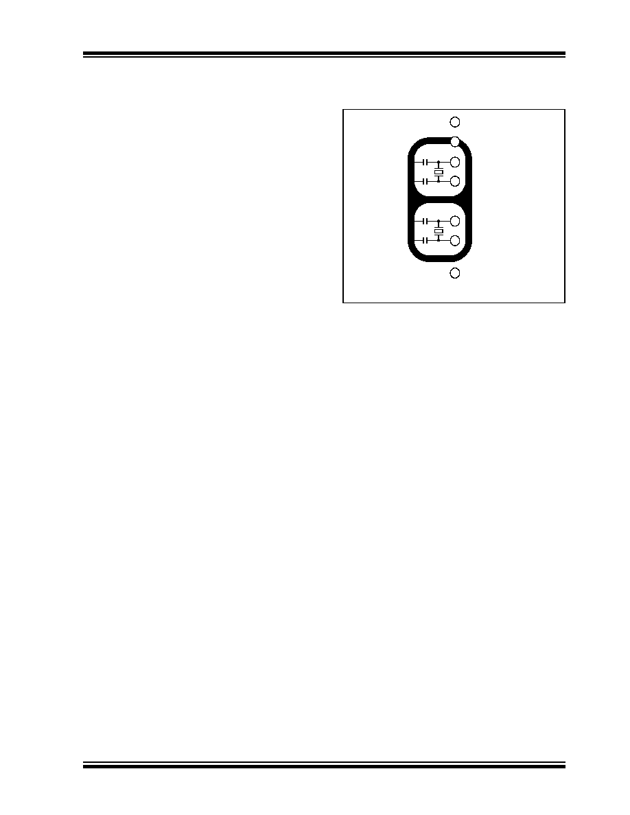
The oscillator circuit, displayed in Figure 13-2, should
be located as close as possible to the microcontroller.
There should be no circuits passing within the oscillator
circuit boundaries other than VSS or VDD.
If a high-speed circuit must be located near the
oscillator (such as the ECCP1 pin in Output Compare
or PWM mode, or the primary oscillator using the
OSC2 pin), a grounded guard ring around the oscillator
circuit, as displayed in Figure 13-3, may be helpful
when used on a single-sided PCB or in addition to a
ground plane.
FIGURE 13-3:
OSCILLATOR CIRCUIT
WITH GROUNDED
GUARD RING
In the low drive level mode, LPT1OSC = 0, it is critical
that RC2 I/O pin signals be kept away from the oscillator
circuit. Configuring RC2 as a digital output, and toggling
it, can potentially disturb the oscillator circuit, even with
relatively good PCB layout. If possible, it is recom-
mended to either leave RC2 unused, or use it as an input
pin with a slew rate limited signal source. If RC2 must be
used as a digital output, it may be necessary to use the
higher drive level oscillator mode (LPT1OSC = 1) with
many PCB layouts. Even in the higher drive level mode,
careful layout procedures should still be followed when
designing the oscillator circuit.
In addition to dV/dt induced noise considerations, it is
also important to ensure that the circuit board is clean.
Even a very small amount of conductive soldering flux
residue can cause PCB leakage currents, which can
overwhelm the oscillator circuit.
13.6
Timer1 Interrupt
The TMR1 register pair (TMR1H:TMR1L) increments
from 0000h to FFFFh and rolls over to 0000h. The
Timer1 interrupt, if enabled, is generated on overflow
which is latched in interrupt flag bit, TMR1IF
(PIR1<0>). This interrupt can be enabled or disabled
by setting or clearing the Timer1 Interrupt Enable bit,
TMR1IE (PIE1<0>).
VDD
OSC1
VSS
OSC2
RC0
RC1
RC2
Note:
Not drawn to scale.
相关PDF资料 |
PDF描述 |
|---|---|
| V375A32E600BL | CONVERTER MOD DC/DC 32V 600W |
| V375A32E600B3 | CONVERTER MOD DC/DC 32V 600W |
| V375A32E600B | CONVERTER MOD DC/DC 32V 600W |
| VE-B2Y-IY-S | CONVERTER MOD DC/DC 3.3V 33W |
| VE-B2Y-IX-S | CONVERTER MOD DC/DC 3.3V 49.5W |
相关代理商/技术参数 |
参数描述 |
|---|---|
| DSPIC30F3012-30I/ML | 功能描述:数字信号处理器和控制器 - DSP, DSC Sensor RoHS:否 制造商:Microchip Technology 核心:dsPIC 数据总线宽度:16 bit 程序存储器大小:16 KB 数据 RAM 大小:2 KB 最大时钟频率:40 MHz 可编程输入/输出端数量:35 定时器数量:3 设备每秒兆指令数:50 MIPs 工作电源电压:3.3 V 最大工作温度:+ 85 C 封装 / 箱体:TQFP-44 安装风格:SMD/SMT |
| DSPIC30F3012-30I/P | 功能描述:数字信号处理器和控制器 - DSP, DSC Sensor RoHS:否 制造商:Microchip Technology 核心:dsPIC 数据总线宽度:16 bit 程序存储器大小:16 KB 数据 RAM 大小:2 KB 最大时钟频率:40 MHz 可编程输入/输出端数量:35 定时器数量:3 设备每秒兆指令数:50 MIPs 工作电源电压:3.3 V 最大工作温度:+ 85 C 封装 / 箱体:TQFP-44 安装风格:SMD/SMT |
| DSPIC30F3012-30I/SO | 功能描述:数字信号处理器和控制器 - DSP, DSC Sensor RoHS:否 制造商:Microchip Technology 核心:dsPIC 数据总线宽度:16 bit 程序存储器大小:16 KB 数据 RAM 大小:2 KB 最大时钟频率:40 MHz 可编程输入/输出端数量:35 定时器数量:3 设备每秒兆指令数:50 MIPs 工作电源电压:3.3 V 最大工作温度:+ 85 C 封装 / 箱体:TQFP-44 安装风格:SMD/SMT |
| dsPIC30F3012T-20E/ML | 功能描述:数字信号处理器和控制器 - DSP, DSC 44LD 20MIPS 24 KB RoHS:否 制造商:Microchip Technology 核心:dsPIC 数据总线宽度:16 bit 程序存储器大小:16 KB 数据 RAM 大小:2 KB 最大时钟频率:40 MHz 可编程输入/输出端数量:35 定时器数量:3 设备每秒兆指令数:50 MIPs 工作电源电压:3.3 V 最大工作温度:+ 85 C 封装 / 箱体:TQFP-44 安装风格:SMD/SMT |
| dsPIC30F3012T-20E/SO | 功能描述:数字信号处理器和控制器 - DSP, DSC 18LD 20MIPS 24 KB RoHS:否 制造商:Microchip Technology 核心:dsPIC 数据总线宽度:16 bit 程序存储器大小:16 KB 数据 RAM 大小:2 KB 最大时钟频率:40 MHz 可编程输入/输出端数量:35 定时器数量:3 设备每秒兆指令数:50 MIPs 工作电源电压:3.3 V 最大工作温度:+ 85 C 封装 / 箱体:TQFP-44 安装风格:SMD/SMT |
发布紧急采购,3分钟左右您将得到回复。