- 您现在的位置:买卖IC网 > PDF目录11347 > DSPIC30F4011T-20E/PT (Microchip Technology)IC DSPIC MCU/DSP 48K 44TQFP PDF资料下载
参数资料
| 型号: | DSPIC30F4011T-20E/PT |
| 厂商: | Microchip Technology |
| 文件页数: | 165/238页 |
| 文件大小: | 0K |
| 描述: | IC DSPIC MCU/DSP 48K 44TQFP |
| 产品培训模块: | Asynchronous Stimulus |
| 标准包装: | 1,200 |
| 系列: | dsPIC™ 30F |
| 核心处理器: | dsPIC |
| 芯体尺寸: | 16-位 |
| 速度: | 20 MIPS |
| 连通性: | CAN,I²C,SPI,UART/USART |
| 外围设备: | 高级欠压探测/复位,电机控制 PWM,QEI,POR,PWM,WDT |
| 输入/输出数: | 30 |
| 程序存储器容量: | 48KB(16K x 24) |
| 程序存储器类型: | 闪存 |
| EEPROM 大小: | 1K x 8 |
| RAM 容量: | 2K x 8 |
| 电压 - 电源 (Vcc/Vdd): | 2.5 V ~ 5.5 V |
| 数据转换器: | A/D 9x10b |
| 振荡器型: | 内部 |
| 工作温度: | -40°C ~ 125°C |
| 封装/外壳: | 44-TQFP |
| 包装: | 带卷 (TR) |
| 其它名称: | DSPIC30F4011T20EP |
第1页第2页第3页第4页第5页第6页第7页第8页第9页第10页第11页第12页第13页第14页第15页第16页第17页第18页第19页第20页第21页第22页第23页第24页第25页第26页第27页第28页第29页第30页第31页第32页第33页第34页第35页第36页第37页第38页第39页第40页第41页第42页第43页第44页第45页第46页第47页第48页第49页第50页第51页第52页第53页第54页第55页第56页第57页第58页第59页第60页第61页第62页第63页第64页第65页第66页第67页第68页第69页第70页第71页第72页第73页第74页第75页第76页第77页第78页第79页第80页第81页第82页第83页第84页第85页第86页第87页第88页第89页第90页第91页第92页第93页第94页第95页第96页第97页第98页第99页第100页第101页第102页第103页第104页第105页第106页第107页第108页第109页第110页第111页第112页第113页第114页第115页第116页第117页第118页第119页第120页第121页第122页第123页第124页第125页第126页第127页第128页第129页第130页第131页第132页第133页第134页第135页第136页第137页第138页第139页第140页第141页第142页第143页第144页第145页第146页第147页第148页第149页第150页第151页第152页第153页第154页第155页第156页第157页第158页第159页第160页第161页第162页第163页第164页当前第165页第166页第167页第168页第169页第170页第171页第172页第173页第174页第175页第176页第177页第178页第179页第180页第181页第182页第183页第184页第185页第186页第187页第188页第189页第190页第191页第192页第193页第194页第195页第196页第197页第198页第199页第200页第201页第202页第203页第204页第205页第206页第207页第208页第209页第210页第211页第212页第213页第214页第215页第216页第217页第218页第219页第220页第221页第222页第223页第224页第225页第226页第227页第228页第229页第230页第231页第232页第233页第234页第235页第236页第237页第238页
dsPIC30F4011/4012
DS70135G-page 32
2010 Microchip Technology Inc.
3.2.2
DATA SPACES
The X data space is used by all instructions and sup-
ports all addressing modes. There are separate read
and write data buses. The X read data bus is the return
data path for all instructions that view data space as
combined X and Y address space. It is also the X
address space data path for the dual operand read
instructions (MAC class). The X write data bus is the
only write path to data space for all instructions.
The X data space also supports Modulo Addressing for
all instructions, subject to addressing mode restric-
tions. Bit-Reversed Addressing is only supported for
writes to X data space.
The Y data space is used in concert with the X data
space by the MAC class of instructions (CLR, ED,
EDAC, MAC, MOVSAC, MPY, MPY.N
and MSC) to pro-
vide two concurrent data read paths. No writes occur
across the Y bus. This class of instructions dedicates
two W register pointers, W10 and W11, to always
address Y data space, independent of X data space,
whereas W8 and W9 always address X data space.
Note that during accumulator write-back, the data
address space is considered a combination of X and Y
data spaces, so the write occurs across the X bus.
Consequently, the write can be to any address in the
entire data space.
The Y data space can only be used for the data
prefetch operation associated with the MAC class of
instructions. It also supports Modulo Addressing for
automated circular buffers. Of course, all other instruc-
tions can access the Y data address space through the
X data path, as part of the composite linear space.
The boundary between the X and Y data spaces is
defined as shown in Figure 3-6 and is not user-
programmable. Should an EA point to data outside its
own assigned address space, or to a location outside
physical memory, an all-zero word/byte is returned. For
example, although Y address space is visible by all
non-MAC instructions using any addressing mode, an
attempt by a MAC instruction to fetch data from that
space, using W8 or W9 (X Space Pointers), returns
0x0000.
All Effective Addresses (EA) are 16 bits wide and point
to bytes within the data space. Therefore, the data
space address range is 64 Kbytes or 32K words.
3.2.3
DATA SPACE WIDTH
The core data width is 16-bits. All internal registers are
organized as 16-bit wide words. Data space memory is
organized in byte addressable, 16-bit wide blocks.
3.2.4
DATA ALIGNMENT
To help maintain backward compatibility with PIC
devices and improve data space memory usage effi-
ciency, the dsPIC30F instruction set supports both
word and byte operations. Data is aligned in data mem-
ory and registers as words, but all data space EAs
resolve to bytes. Data byte reads read the complete
word, which contains the byte, using the LSb of any EA
to determine which byte to select. The selected byte is
placed onto the LSB of the X data path (no byte
accesses are possible from the Y data path as the MAC
class of instructions can only fetch words). That is, data
memory and registers are organized as two parallel
byte-wide entities, with shared (word) address decode,
but separate write lines. Data byte writes only write to
the corresponding side of the array or register which
matches the byte address.
As a consequence of this byte accessibility, all Effective
Address calculations (including those generated by the
DSP operations, which are restricted to word-sized
data) are internally scaled to step through word-aligned
memory. For example, the core would recognize that
Post-Modified Register Indirect Addressing mode,
[Ws++], will result in a value of Ws + 1 for byte
operations and Ws + 2 for word operations.
All word accesses must be aligned to an even address.
Misaligned word data fetches are not supported, so
care must be taken when mixing byte and word opera-
tions, or translating from 8-bit MCU code. Should a
misaligned read or write be attempted, an address
error trap is generated. If the error occurred on a read,
the instruction underway is completed, whereas if it
occurred on a write, the instruction will be executed but
the write does not occur. In either case, a trap is then
executed, allowing the system and/or user to examine
the machine state prior to execution of the address
Fault.
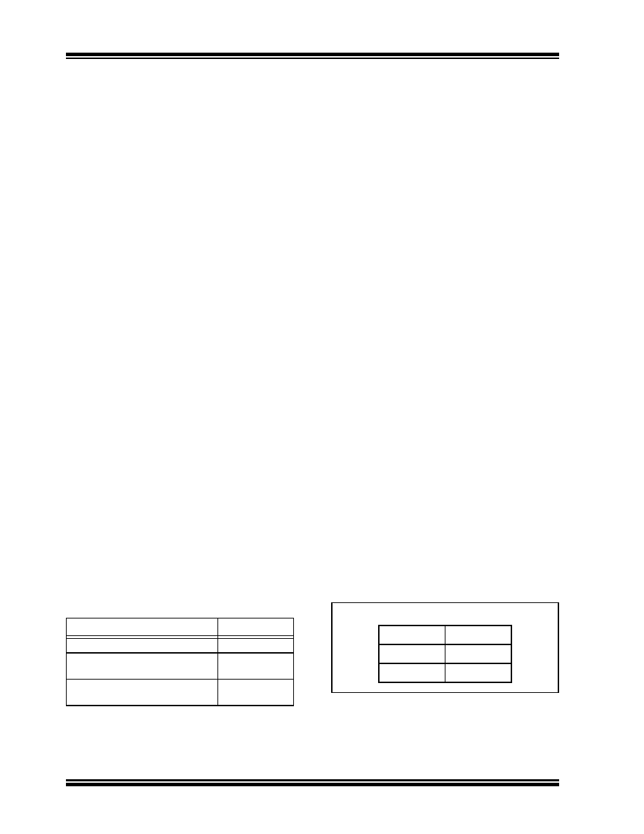
FIGURE 3-8:
DATA ALIGNMENT
TABLE 3-2:
EFFECT OF INVALID
MEMORY ACCESSES
Attempted Operation
Data Returned
EA = an unimplemented address
0x0000
W8 or W9 used to access Y data
space in a MAC instruction
0x0000
W10 or W11 used to access X
data space in a MAC instruction
0x0000
15
8 7
0
0001
0003
0005
0000
0002
0004
Byte 1
Byte 0
Byte 3
Byte 2
Byte 5
Byte 4
LSB
MSB
相关PDF资料 |
PDF描述 |
|---|---|
| GRM3166T1H221JD01D | CAP CER 220PF 50V 5% T2H 1206 |
| GRM3166R1H181JZ01D | CAP CER 180PF 50V 5% R2H 1206 |
| PIC16C62A-10I/SO | IC MCU OTP 2KX14 PWM 28SOIC |
| GRM3166P1H181JZ01D | CAP CER 180PF 50V 5% P2H 1206 |
| PIC16C62A-20I/SO | IC MCU OTP 2KX14 PWM 28SOIC |
相关代理商/技术参数 |
参数描述 |
|---|---|
| DSPIC30F4011T-20I/ML | 功能描述:数字信号处理器和控制器 - DSP, DSC DIG SIG CONTR RoHS:否 制造商:Microchip Technology 核心:dsPIC 数据总线宽度:16 bit 程序存储器大小:16 KB 数据 RAM 大小:2 KB 最大时钟频率:40 MHz 可编程输入/输出端数量:35 定时器数量:3 设备每秒兆指令数:50 MIPs 工作电源电压:3.3 V 最大工作温度:+ 85 C 封装 / 箱体:TQFP-44 安装风格:SMD/SMT |
| DSPIC30F4011T-20I/PT | 功能描述:数字信号处理器和控制器 - DSP, DSC 16 Bit MCU/DSP 20M 48KB FL RoHS:否 制造商:Microchip Technology 核心:dsPIC 数据总线宽度:16 bit 程序存储器大小:16 KB 数据 RAM 大小:2 KB 最大时钟频率:40 MHz 可编程输入/输出端数量:35 定时器数量:3 设备每秒兆指令数:50 MIPs 工作电源电压:3.3 V 最大工作温度:+ 85 C 封装 / 箱体:TQFP-44 安装风格:SMD/SMT |
| DSPIC30F4011T-30I/ML | 功能描述:数字信号处理器和控制器 - DSP, DSC 16 Bit MCU/DSP 44LD 30M 48KB FL RoHS:否 制造商:Microchip Technology 核心:dsPIC 数据总线宽度:16 bit 程序存储器大小:16 KB 数据 RAM 大小:2 KB 最大时钟频率:40 MHz 可编程输入/输出端数量:35 定时器数量:3 设备每秒兆指令数:50 MIPs 工作电源电压:3.3 V 最大工作温度:+ 85 C 封装 / 箱体:TQFP-44 安装风格:SMD/SMT |
| DSPIC30F4011T-30I/PT | 功能描述:数字信号处理器和控制器 - DSP, DSC 16 Bit MCU/DSP 30M 48KB FL RoHS:否 制造商:Microchip Technology 核心:dsPIC 数据总线宽度:16 bit 程序存储器大小:16 KB 数据 RAM 大小:2 KB 最大时钟频率:40 MHz 可编程输入/输出端数量:35 定时器数量:3 设备每秒兆指令数:50 MIPs 工作电源电压:3.3 V 最大工作温度:+ 85 C 封装 / 箱体:TQFP-44 安装风格:SMD/SMT |
| dsPIC30F4012-20E/ML | 功能描述:数字信号处理器和控制器 - DSP, DSC 44LD 20MIPS 48 KB RoHS:否 制造商:Microchip Technology 核心:dsPIC 数据总线宽度:16 bit 程序存储器大小:16 KB 数据 RAM 大小:2 KB 最大时钟频率:40 MHz 可编程输入/输出端数量:35 定时器数量:3 设备每秒兆指令数:50 MIPs 工作电源电压:3.3 V 最大工作温度:+ 85 C 封装 / 箱体:TQFP-44 安装风格:SMD/SMT |
发布紧急采购,3分钟左右您将得到回复。