- 您现在的位置:买卖IC网 > PDF目录11347 > DSPIC30F4011T-20E/PT (Microchip Technology)IC DSPIC MCU/DSP 48K 44TQFP PDF资料下载
参数资料
| 型号: | DSPIC30F4011T-20E/PT |
| 厂商: | Microchip Technology |
| 文件页数: | 178/238页 |
| 文件大小: | 0K |
| 描述: | IC DSPIC MCU/DSP 48K 44TQFP |
| 产品培训模块: | Asynchronous Stimulus |
| 标准包装: | 1,200 |
| 系列: | dsPIC™ 30F |
| 核心处理器: | dsPIC |
| 芯体尺寸: | 16-位 |
| 速度: | 20 MIPS |
| 连通性: | CAN,I²C,SPI,UART/USART |
| 外围设备: | 高级欠压探测/复位,电机控制 PWM,QEI,POR,PWM,WDT |
| 输入/输出数: | 30 |
| 程序存储器容量: | 48KB(16K x 24) |
| 程序存储器类型: | 闪存 |
| EEPROM 大小: | 1K x 8 |
| RAM 容量: | 2K x 8 |
| 电压 - 电源 (Vcc/Vdd): | 2.5 V ~ 5.5 V |
| 数据转换器: | A/D 9x10b |
| 振荡器型: | 内部 |
| 工作温度: | -40°C ~ 125°C |
| 封装/外壳: | 44-TQFP |
| 包装: | 带卷 (TR) |
| 其它名称: | DSPIC30F4011T20EP |
第1页第2页第3页第4页第5页第6页第7页第8页第9页第10页第11页第12页第13页第14页第15页第16页第17页第18页第19页第20页第21页第22页第23页第24页第25页第26页第27页第28页第29页第30页第31页第32页第33页第34页第35页第36页第37页第38页第39页第40页第41页第42页第43页第44页第45页第46页第47页第48页第49页第50页第51页第52页第53页第54页第55页第56页第57页第58页第59页第60页第61页第62页第63页第64页第65页第66页第67页第68页第69页第70页第71页第72页第73页第74页第75页第76页第77页第78页第79页第80页第81页第82页第83页第84页第85页第86页第87页第88页第89页第90页第91页第92页第93页第94页第95页第96页第97页第98页第99页第100页第101页第102页第103页第104页第105页第106页第107页第108页第109页第110页第111页第112页第113页第114页第115页第116页第117页第118页第119页第120页第121页第122页第123页第124页第125页第126页第127页第128页第129页第130页第131页第132页第133页第134页第135页第136页第137页第138页第139页第140页第141页第142页第143页第144页第145页第146页第147页第148页第149页第150页第151页第152页第153页第154页第155页第156页第157页第158页第159页第160页第161页第162页第163页第164页第165页第166页第167页第168页第169页第170页第171页第172页第173页第174页第175页第176页第177页当前第178页第179页第180页第181页第182页第183页第184页第185页第186页第187页第188页第189页第190页第191页第192页第193页第194页第195页第196页第197页第198页第199页第200页第201页第202页第203页第204页第205页第206页第207页第208页第209页第210页第211页第212页第213页第214页第215页第216页第217页第218页第219页第220页第221页第222页第223页第224页第225页第226页第227页第228页第229页第230页第231页第232页第233页第234页第235页第236页第237页第238页
dsPIC30F4011/4012
DS70135G-page 44
2010 Microchip Technology Inc.
5.1
Interrupt Priority
The user-assignable Interrupt Priority (IP<2:0>) bits for
each individual interrupt source are located in the Least
Significant 3 bits of each nibble within the IPCx regis-
ter(s). Bit 3 of each nibble is not used and is read as a
‘0’. These bits define the priority level assigned to a
particular interrupt by the user.
Since more than one interrupt request source may be
assigned to a specific user-assigned priority level, a
means is provided to assign priority within a given level.
This method is called “Natural Order Priority”.
Natural order priority is determined by the position of
an interrupt in the vector table, and only affects
interrupt operation when multiple interrupts with the
same user-assigned priority become pending at the
same time.
Table 5-1 lists the interrupt numbers and interrupt
sources for the dsPIC DSCs and their associated
vector numbers.
The ability for the user to assign every interrupt to one
of seven priority levels implies that the user can assign
a very high overall priority level to an interrupt with a
low natural order priority. For example, the PLVD (Low-
Voltage Detect) can be given a priority of 7. The INT0
(External Interrupt 0) may be assigned to priority
level 1, thus giving it a very low effective priority.
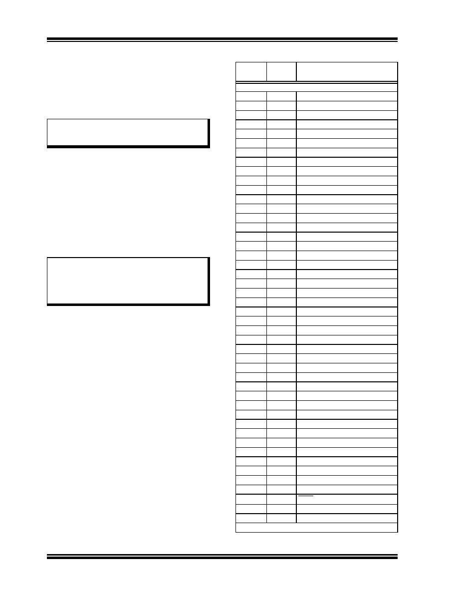
TABLE 5-1:
INTERRUPT VECTOR TABLE
Note:
The user-assignable priority levels start at
0 as the lowest priority, and level 7 as the
highest priority.
Note 1: The natural order priority scheme has 0
as the highest priority and 53 as the
lowest priority.
2: The natural order priority number is the
same as the INT number.
INT
Number
Vector
Number
Interrupt Source
Highest Natural Order Priority
0
8
INT0 – External Interrupt 0
1
9
IC1 – Input Capture 1
2
10
OC1 – Output Compare 1
3
11
T1 – Timer1
4
12
IC2 – Input Capture 2
5
13
OC2 – Output Compare 2
6
14
T2 – Timer2
7
15
T3 – Timer3
816
SPI1
9
17
U1RX – UART1 Receiver
10
18
U1TX – UART1 Transmitter
11
19
ADC – ADC Convert Done
12
20
NVM – NVM Write Complete
13
21
SI2C – I2C Slave Interrupt
14
22
MI2C – I2C Master Interrupt
15
23
Input Change Interrupt
16
24
INT1 – External Interrupt 1
17
25
IC7 – Input Capture 7
18
26
IC8 – Input Capture 8
19
27
OC3 – Output Compare 3
20
28
OC4 – Output Compare 4
21
29
T4 – Timer4
22
30
T5 – Timer5
23
31
INT2 – External Interrupt 2
24
32
U2RX – UART2 Receiver
25
33
U2TX – UART2 Transmitter
26
34
Reserved
27
35
C1 – Combined IRQ for CAN1
28
36
Reserved
29
37
Reserved
30
38
Reserved
31
39
Reserved
32
40
Reserved
33
41
Reserved
34
42
Reserved
35
43
Reserved
36
44
Reserved
37
45
Reserved
38
46
Reserved
39
47
PWM – PWM Period Match
40
48
QEI – QEI Interrupt
41
49
Reserved
42
50
Reserved
43
51
FLTA – PWM Fault A
44
52
Reserved
45-53
53-61
Reserved
Lowest Natural Order Priority
相关PDF资料 |
PDF描述 |
|---|---|
| GRM3166T1H221JD01D | CAP CER 220PF 50V 5% T2H 1206 |
| GRM3166R1H181JZ01D | CAP CER 180PF 50V 5% R2H 1206 |
| PIC16C62A-10I/SO | IC MCU OTP 2KX14 PWM 28SOIC |
| GRM3166P1H181JZ01D | CAP CER 180PF 50V 5% P2H 1206 |
| PIC16C62A-20I/SO | IC MCU OTP 2KX14 PWM 28SOIC |
相关代理商/技术参数 |
参数描述 |
|---|---|
| DSPIC30F4011T-20I/ML | 功能描述:数字信号处理器和控制器 - DSP, DSC DIG SIG CONTR RoHS:否 制造商:Microchip Technology 核心:dsPIC 数据总线宽度:16 bit 程序存储器大小:16 KB 数据 RAM 大小:2 KB 最大时钟频率:40 MHz 可编程输入/输出端数量:35 定时器数量:3 设备每秒兆指令数:50 MIPs 工作电源电压:3.3 V 最大工作温度:+ 85 C 封装 / 箱体:TQFP-44 安装风格:SMD/SMT |
| DSPIC30F4011T-20I/PT | 功能描述:数字信号处理器和控制器 - DSP, DSC 16 Bit MCU/DSP 20M 48KB FL RoHS:否 制造商:Microchip Technology 核心:dsPIC 数据总线宽度:16 bit 程序存储器大小:16 KB 数据 RAM 大小:2 KB 最大时钟频率:40 MHz 可编程输入/输出端数量:35 定时器数量:3 设备每秒兆指令数:50 MIPs 工作电源电压:3.3 V 最大工作温度:+ 85 C 封装 / 箱体:TQFP-44 安装风格:SMD/SMT |
| DSPIC30F4011T-30I/ML | 功能描述:数字信号处理器和控制器 - DSP, DSC 16 Bit MCU/DSP 44LD 30M 48KB FL RoHS:否 制造商:Microchip Technology 核心:dsPIC 数据总线宽度:16 bit 程序存储器大小:16 KB 数据 RAM 大小:2 KB 最大时钟频率:40 MHz 可编程输入/输出端数量:35 定时器数量:3 设备每秒兆指令数:50 MIPs 工作电源电压:3.3 V 最大工作温度:+ 85 C 封装 / 箱体:TQFP-44 安装风格:SMD/SMT |
| DSPIC30F4011T-30I/PT | 功能描述:数字信号处理器和控制器 - DSP, DSC 16 Bit MCU/DSP 30M 48KB FL RoHS:否 制造商:Microchip Technology 核心:dsPIC 数据总线宽度:16 bit 程序存储器大小:16 KB 数据 RAM 大小:2 KB 最大时钟频率:40 MHz 可编程输入/输出端数量:35 定时器数量:3 设备每秒兆指令数:50 MIPs 工作电源电压:3.3 V 最大工作温度:+ 85 C 封装 / 箱体:TQFP-44 安装风格:SMD/SMT |
| dsPIC30F4012-20E/ML | 功能描述:数字信号处理器和控制器 - DSP, DSC 44LD 20MIPS 48 KB RoHS:否 制造商:Microchip Technology 核心:dsPIC 数据总线宽度:16 bit 程序存储器大小:16 KB 数据 RAM 大小:2 KB 最大时钟频率:40 MHz 可编程输入/输出端数量:35 定时器数量:3 设备每秒兆指令数:50 MIPs 工作电源电压:3.3 V 最大工作温度:+ 85 C 封装 / 箱体:TQFP-44 安装风格:SMD/SMT |
发布紧急采购,3分钟左右您将得到回复。