- 您现在的位置:买卖IC网 > PDF目录11347 > DSPIC30F4011T-20E/PT (Microchip Technology)IC DSPIC MCU/DSP 48K 44TQFP PDF资料下载
参数资料
| 型号: | DSPIC30F4011T-20E/PT |
| 厂商: | Microchip Technology |
| 文件页数: | 54/238页 |
| 文件大小: | 0K |
| 描述: | IC DSPIC MCU/DSP 48K 44TQFP |
| 产品培训模块: | Asynchronous Stimulus |
| 标准包装: | 1,200 |
| 系列: | dsPIC™ 30F |
| 核心处理器: | dsPIC |
| 芯体尺寸: | 16-位 |
| 速度: | 20 MIPS |
| 连通性: | CAN,I²C,SPI,UART/USART |
| 外围设备: | 高级欠压探测/复位,电机控制 PWM,QEI,POR,PWM,WDT |
| 输入/输出数: | 30 |
| 程序存储器容量: | 48KB(16K x 24) |
| 程序存储器类型: | 闪存 |
| EEPROM 大小: | 1K x 8 |
| RAM 容量: | 2K x 8 |
| 电压 - 电源 (Vcc/Vdd): | 2.5 V ~ 5.5 V |
| 数据转换器: | A/D 9x10b |
| 振荡器型: | 内部 |
| 工作温度: | -40°C ~ 125°C |
| 封装/外壳: | 44-TQFP |
| 包装: | 带卷 (TR) |
| 其它名称: | DSPIC30F4011T20EP |
第1页第2页第3页第4页第5页第6页第7页第8页第9页第10页第11页第12页第13页第14页第15页第16页第17页第18页第19页第20页第21页第22页第23页第24页第25页第26页第27页第28页第29页第30页第31页第32页第33页第34页第35页第36页第37页第38页第39页第40页第41页第42页第43页第44页第45页第46页第47页第48页第49页第50页第51页第52页第53页当前第54页第55页第56页第57页第58页第59页第60页第61页第62页第63页第64页第65页第66页第67页第68页第69页第70页第71页第72页第73页第74页第75页第76页第77页第78页第79页第80页第81页第82页第83页第84页第85页第86页第87页第88页第89页第90页第91页第92页第93页第94页第95页第96页第97页第98页第99页第100页第101页第102页第103页第104页第105页第106页第107页第108页第109页第110页第111页第112页第113页第114页第115页第116页第117页第118页第119页第120页第121页第122页第123页第124页第125页第126页第127页第128页第129页第130页第131页第132页第133页第134页第135页第136页第137页第138页第139页第140页第141页第142页第143页第144页第145页第146页第147页第148页第149页第150页第151页第152页第153页第154页第155页第156页第157页第158页第159页第160页第161页第162页第163页第164页第165页第166页第167页第168页第169页第170页第171页第172页第173页第174页第175页第176页第177页第178页第179页第180页第181页第182页第183页第184页第185页第186页第187页第188页第189页第190页第191页第192页第193页第194页第195页第196页第197页第198页第199页第200页第201页第202页第203页第204页第205页第206页第207页第208页第209页第210页第211页第212页第213页第214页第215页第216页第217页第218页第219页第220页第221页第222页第223页第224页第225页第226页第227页第228页第229页第230页第231页第232页第233页第234页第235页第236页第237页第238页
2010 Microchip Technology Inc.
DS70135G-page 147
dsPIC30F4011/4012
20.9
Module Power-Down Modes
The module has 3 internal power modes. When the
ADON bit is ‘1’, the module is in Active mode; it is fully
powered and functional. When ADON is ‘0’, the module
is in Off mode. The digital and analog portions of the
circuit are disabled for maximum current savings. In
order to return to the Active mode from Off mode, the
user must wait for the ADC circuitry to stabilize.
20.10 A/D Operation During CPU Sleep
and Idle Modes
20.10.1
A/D OPERATION DURING CPU
SLEEP MODE
When the device enters Sleep mode, all clock sources
to the module are shut down and stay at logic ‘0’.
If Sleep occurs in the middle of a conversion, the
conversion is aborted. The converter will not continue
with a partially completed conversion on exit from
Sleep mode.
Register contents are not affected by the device
entering or leaving Sleep mode.
The ADC module can operate during Sleep mode if the
A/D clock source is set to RC (ADRC = 1). When the
RC clock source is selected, the ADC module waits
one instruction cycle before starting the conversion.
This allows the SLEEP instruction to be executed,
which eliminates all digital switching noise from the
conversion. When the conversion is complete, the
DONE bit is set and the result is loaded into the
ADCBUFx register.
If the A/D interrupt is enabled, the device wakes up
from Sleep. If the A/D interrupt is not enabled, the ADC
module is then turned off, although the ADON bit
remains set.
20.10.2
A/D OPERATION DURING CPU IDLE
MODE
The ADSIDL bit selects if the module stops on Idle or
continues on Idle. If ADSIDL = 0, the module continues
operation on assertion of Idle mode. If ADSIDL = 1, the
module stops on Idle.
20.11 Effects of a Reset
A device Reset forces all registers to their Reset state.
This forces the ADC module to be turned off, and any
conversion and acquisition sequence is aborted. The
values that are in the ADCBUFx registers are not
modified. The A/D Result register contains unknown
data after a Power-on Reset.
20.12 Output Formats
The A/D result is 10 bits wide. The data buffer RAM is
also 10 bits wide. The 10-bit data can be read in one of
four different formats. The FORM<1:0> bits select the
format. Each of the output formats translates to a 16-bit
result on the data bus.
Write data will always be in right justified (integer)
format.
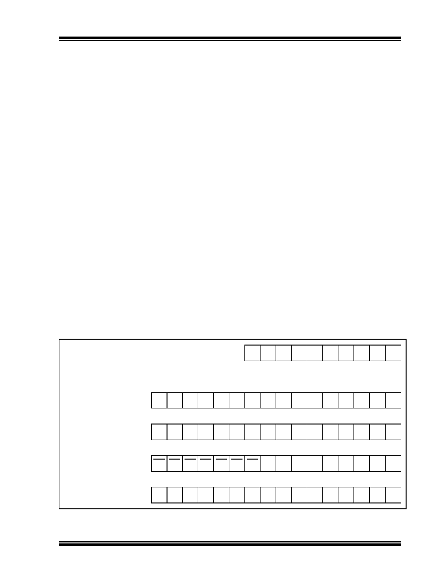
FIGURE 20-4:
A/D OUTPUT DATA FORMATS
RAM Contents:
d09 d08 d07 d06 d05 d04 d03 d02 d01 d00
Read to Bus:
Signed Fractional (1.15)
d09 d08 d07 d06 d05 d04 d03 d02 d01 d00
000000
Fractional (1.15)
d09 d08 d07 d06 d05 d04 d03 d02 d01 d00
000000
Signed Integer
d09 d09 d09 d09 d09 d09 d09 d08 d07 d06 d05 d04 d03 d02 d01 d00
Integer
0
d09 d08 d07 d06 d05 d04 d03 d02 d01 d00
相关PDF资料 |
PDF描述 |
|---|---|
| GRM3166T1H221JD01D | CAP CER 220PF 50V 5% T2H 1206 |
| GRM3166R1H181JZ01D | CAP CER 180PF 50V 5% R2H 1206 |
| PIC16C62A-10I/SO | IC MCU OTP 2KX14 PWM 28SOIC |
| GRM3166P1H181JZ01D | CAP CER 180PF 50V 5% P2H 1206 |
| PIC16C62A-20I/SO | IC MCU OTP 2KX14 PWM 28SOIC |
相关代理商/技术参数 |
参数描述 |
|---|---|
| DSPIC30F4011T-20I/ML | 功能描述:数字信号处理器和控制器 - DSP, DSC DIG SIG CONTR RoHS:否 制造商:Microchip Technology 核心:dsPIC 数据总线宽度:16 bit 程序存储器大小:16 KB 数据 RAM 大小:2 KB 最大时钟频率:40 MHz 可编程输入/输出端数量:35 定时器数量:3 设备每秒兆指令数:50 MIPs 工作电源电压:3.3 V 最大工作温度:+ 85 C 封装 / 箱体:TQFP-44 安装风格:SMD/SMT |
| DSPIC30F4011T-20I/PT | 功能描述:数字信号处理器和控制器 - DSP, DSC 16 Bit MCU/DSP 20M 48KB FL RoHS:否 制造商:Microchip Technology 核心:dsPIC 数据总线宽度:16 bit 程序存储器大小:16 KB 数据 RAM 大小:2 KB 最大时钟频率:40 MHz 可编程输入/输出端数量:35 定时器数量:3 设备每秒兆指令数:50 MIPs 工作电源电压:3.3 V 最大工作温度:+ 85 C 封装 / 箱体:TQFP-44 安装风格:SMD/SMT |
| DSPIC30F4011T-30I/ML | 功能描述:数字信号处理器和控制器 - DSP, DSC 16 Bit MCU/DSP 44LD 30M 48KB FL RoHS:否 制造商:Microchip Technology 核心:dsPIC 数据总线宽度:16 bit 程序存储器大小:16 KB 数据 RAM 大小:2 KB 最大时钟频率:40 MHz 可编程输入/输出端数量:35 定时器数量:3 设备每秒兆指令数:50 MIPs 工作电源电压:3.3 V 最大工作温度:+ 85 C 封装 / 箱体:TQFP-44 安装风格:SMD/SMT |
| DSPIC30F4011T-30I/PT | 功能描述:数字信号处理器和控制器 - DSP, DSC 16 Bit MCU/DSP 30M 48KB FL RoHS:否 制造商:Microchip Technology 核心:dsPIC 数据总线宽度:16 bit 程序存储器大小:16 KB 数据 RAM 大小:2 KB 最大时钟频率:40 MHz 可编程输入/输出端数量:35 定时器数量:3 设备每秒兆指令数:50 MIPs 工作电源电压:3.3 V 最大工作温度:+ 85 C 封装 / 箱体:TQFP-44 安装风格:SMD/SMT |
| dsPIC30F4012-20E/ML | 功能描述:数字信号处理器和控制器 - DSP, DSC 44LD 20MIPS 48 KB RoHS:否 制造商:Microchip Technology 核心:dsPIC 数据总线宽度:16 bit 程序存储器大小:16 KB 数据 RAM 大小:2 KB 最大时钟频率:40 MHz 可编程输入/输出端数量:35 定时器数量:3 设备每秒兆指令数:50 MIPs 工作电源电压:3.3 V 最大工作温度:+ 85 C 封装 / 箱体:TQFP-44 安装风格:SMD/SMT |
发布紧急采购,3分钟左右您将得到回复。