- 您现在的位置:买卖IC网 > PDF目录11342 > DSPIC30F4012-20E/ML (Microchip Technology)IC DSPIC MCU/DSP 48K 44QFN PDF资料下载
参数资料
| 型号: | DSPIC30F4012-20E/ML |
| 厂商: | Microchip Technology |
| 文件页数: | 29/66页 |
| 文件大小: | 0K |
| 描述: | IC DSPIC MCU/DSP 48K 44QFN |
| 产品培训模块: | Asynchronous Stimulus |
| 标准包装: | 45 |
| 系列: | dsPIC™ 30F |
| 核心处理器: | dsPIC |
| 芯体尺寸: | 16-位 |
| 速度: | 20 MIPS |
| 连通性: | CAN,I²C,SPI,UART/USART |
| 外围设备: | 高级欠压探测/复位,电机控制 PWM,QEI,POR,PWM,WDT |
| 输入/输出数: | 20 |
| 程序存储器容量: | 48KB(16K x 24) |
| 程序存储器类型: | 闪存 |
| EEPROM 大小: | 1K x 8 |
| RAM 容量: | 2K x 8 |
| 电压 - 电源 (Vcc/Vdd): | 2.5 V ~ 5.5 V |
| 数据转换器: | A/D 6x10b |
| 振荡器型: | 内部 |
| 工作温度: | -40°C ~ 125°C |
| 封装/外壳: | 44-VQFN 裸露焊盘 |
| 包装: | 管件 |
| 配用: | XLT44QFN4-ND - SOCKET TRANS ICE 28DIP TO 44QFN |
| 其它名称: | DSPIC30F401220EML |
第1页第2页第3页第4页第5页第6页第7页第8页第9页第10页第11页第12页第13页第14页第15页第16页第17页第18页第19页第20页第21页第22页第23页第24页第25页第26页第27页第28页当前第29页第30页第31页第32页第33页第34页第35页第36页第37页第38页第39页第40页第41页第42页第43页第44页第45页第46页第47页第48页第49页第50页第51页第52页第53页第54页第55页第56页第57页第58页第59页第60页第61页第62页第63页第64页第65页第66页
2010 Microchip Technology Inc.
DS70102K-page 35
dsPIC30F Flash Programming Specification
11.2.2
REGOUT SERIAL INSTRUCTION
EXECUTION
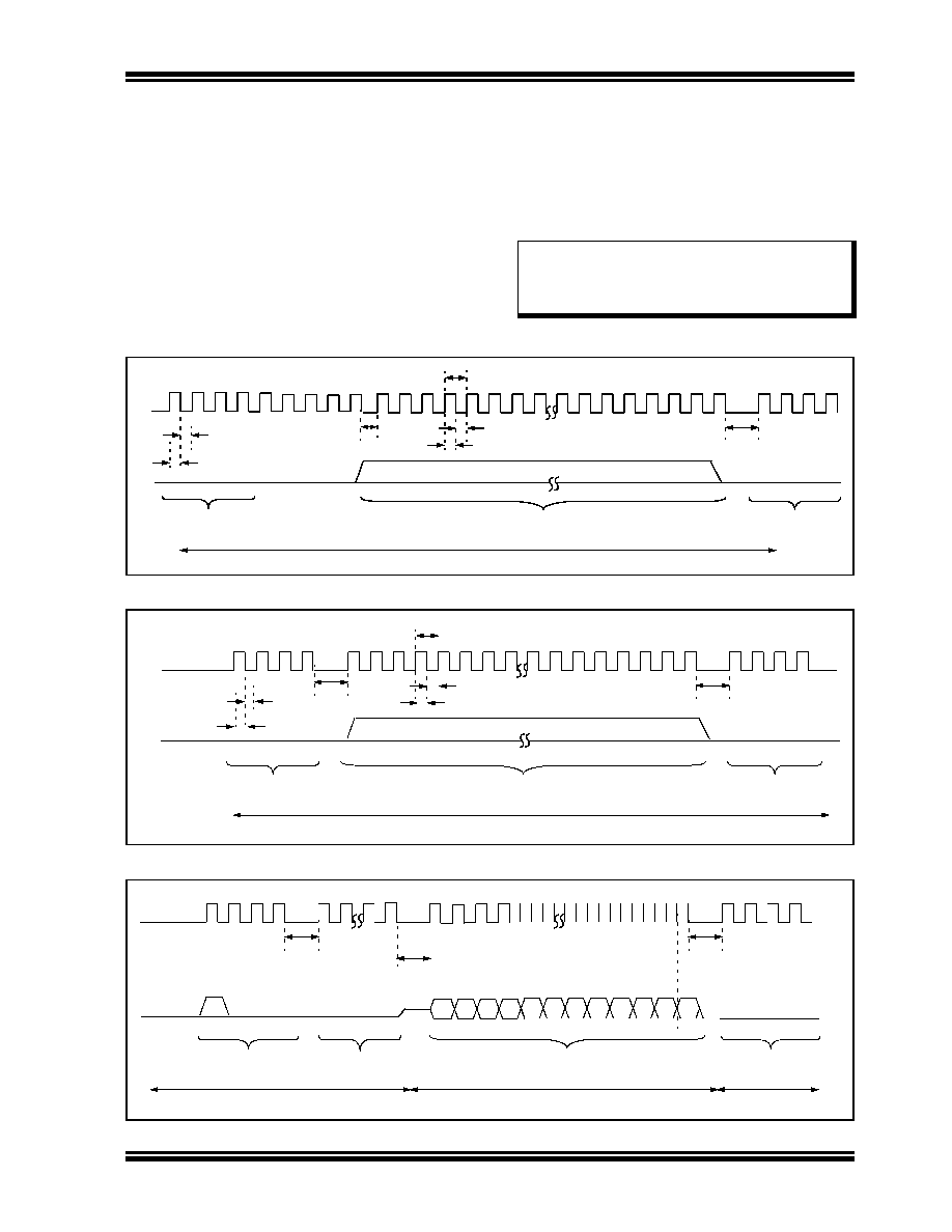
The REGOUT control code allows for data to be
extracted from the device in ICSP mode. It is used to
clock the contents of the VISI register out of the device
over the PGD pin. Once the REGOUT control code is
received, eight clock cycles are required to process the
command. During this time, the CPU is held idle. After
these eight cycles, an additional 16 cycles are required
to clock the data out (see Figure 11-3).
The REGOUT instruction is unique because the PGD
pin is an input when the control code is transmitted to
the device. However, once the control code is
processed, the PGD pin becomes an output as the VISI
register is shifted out. After the contents of the VISI are
shifted out, PGD becomes an input again as the state
machine holds the CPU idle until the next 4-bit control
code is shifted in.
Note:
Once the contents of VISI are shifted out,
the dsPIC DSC device maintains PGD
as an output until the first rising edge of
the next clock is received.
FIGURE 11-1:
PROGRAM ENTRY AFTER RESET
FIGURE 11-2:
SIX SERIAL EXECUTION
FIGURE 11-3:
REGOUT SERIAL EXECUTION
P4
23
12
3
23 24
1
2
3
4
P1
PGC
P4a
PGD
24-bit Instruction Fetch
Execute 24-bit Instruction,
Execute PC – 1,
14
00
0
Fetch SIX Control Code
Fetch Next Control Code
4
5
6
7
8
18 19 202122
17
LSB X
X
X MSB
PGD = Input
P2
P3
P1B
P1A
56
7
00
0
00
0
89
00
P4
23
1
2
3
23 24
1
2
3
4
P1
PGC
P4a
PGD
24-bit Instruction Fetch
Execute 24-bit Instruction,
Execute PC – 1,
14
00
0
00
0
Fetch SIX Control Code
Fetch Next Control Code
4
5
6
7
8
18 19 202122
17
LSB X
X
X MSB
PGD = Input
P2
P3
P1a
P1b
12
3
4
1
2
7
8
PGC
P4
PGD
PGD = Input
Execute Previous Instruction,
CPU Held In Idle
Shift Out VISI Register <15:0>
P5
PGD = Output
12
3
12
3
4
P4a
11
13
15 16
14
12
No Execution Takes Place,
Fetch Next Control Code
0
00
0
PGD = Input
MSb
1
2
3
4
1
45
6
LSb
14
13
12
...
11
10
0
Fetch REGOUT Control Code
0
相关PDF资料 |
PDF描述 |
|---|---|
| VI-271-IY-S | CONVERTER MOD DC/DC 12V 50W |
| MC14551BCPG | IC MUX/DEMUX QUAD 2X1 16DIP |
| VI-25K-IY-S | CONVERTER MOD DC/DC 40V 50W |
| ISL84544CPZ | IC SWITCH SPDT 8DIP |
| VI-25J-IY-S | CONVERTER MOD DC/DC 36V 50W |
相关代理商/技术参数 |
参数描述 |
|---|---|
| dsPIC30F4012-20I/ML | 功能描述:数字信号处理器和控制器 - DSP, DSC 44LD 20MIPS 48 KB RoHS:否 制造商:Microchip Technology 核心:dsPIC 数据总线宽度:16 bit 程序存储器大小:16 KB 数据 RAM 大小:2 KB 最大时钟频率:40 MHz 可编程输入/输出端数量:35 定时器数量:3 设备每秒兆指令数:50 MIPs 工作电源电压:3.3 V 最大工作温度:+ 85 C 封装 / 箱体:TQFP-44 安装风格:SMD/SMT |
| DSPIC30F4012-20I/SO | 功能描述:数字信号处理器和控制器 - DSP, DSC 16 Bit MCU/DSP 28LD 20M 48KB FL RoHS:否 制造商:Microchip Technology 核心:dsPIC 数据总线宽度:16 bit 程序存储器大小:16 KB 数据 RAM 大小:2 KB 最大时钟频率:40 MHz 可编程输入/输出端数量:35 定时器数量:3 设备每秒兆指令数:50 MIPs 工作电源电压:3.3 V 最大工作温度:+ 85 C 封装 / 箱体:TQFP-44 安装风格:SMD/SMT |
| DSPIC30F4012-20I/SP | 功能描述:数字信号处理器和控制器 - DSP, DSC 16 Bit MCU/DSP 28LD 20M 48KB FL RoHS:否 制造商:Microchip Technology 核心:dsPIC 数据总线宽度:16 bit 程序存储器大小:16 KB 数据 RAM 大小:2 KB 最大时钟频率:40 MHz 可编程输入/输出端数量:35 定时器数量:3 设备每秒兆指令数:50 MIPs 工作电源电压:3.3 V 最大工作温度:+ 85 C 封装 / 箱体:TQFP-44 安装风格:SMD/SMT |
| DSPIC30F4012-20I/SP | 制造商:Microchip Technology Inc 功能描述:16BIT MCU-DSP 20MHZ 30F4012 SDIL |
| DSPIC30F4012-30I/ML | 功能描述:数字信号处理器和控制器 - DSP, DSC Motor Control RoHS:否 制造商:Microchip Technology 核心:dsPIC 数据总线宽度:16 bit 程序存储器大小:16 KB 数据 RAM 大小:2 KB 最大时钟频率:40 MHz 可编程输入/输出端数量:35 定时器数量:3 设备每秒兆指令数:50 MIPs 工作电源电压:3.3 V 最大工作温度:+ 85 C 封装 / 箱体:TQFP-44 安装风格:SMD/SMT |
发布紧急采购,3分钟左右您将得到回复。