- 您现在的位置:买卖IC网 > PDF目录11342 > DSPIC30F4012-20E/ML (Microchip Technology)IC DSPIC MCU/DSP 48K 44QFN PDF资料下载
参数资料
| 型号: | DSPIC30F4012-20E/ML |
| 厂商: | Microchip Technology |
| 文件页数: | 31/66页 |
| 文件大小: | 0K |
| 描述: | IC DSPIC MCU/DSP 48K 44QFN |
| 产品培训模块: | Asynchronous Stimulus |
| 标准包装: | 45 |
| 系列: | dsPIC™ 30F |
| 核心处理器: | dsPIC |
| 芯体尺寸: | 16-位 |
| 速度: | 20 MIPS |
| 连通性: | CAN,I²C,SPI,UART/USART |
| 外围设备: | 高级欠压探测/复位,电机控制 PWM,QEI,POR,PWM,WDT |
| 输入/输出数: | 20 |
| 程序存储器容量: | 48KB(16K x 24) |
| 程序存储器类型: | 闪存 |
| EEPROM 大小: | 1K x 8 |
| RAM 容量: | 2K x 8 |
| 电压 - 电源 (Vcc/Vdd): | 2.5 V ~ 5.5 V |
| 数据转换器: | A/D 6x10b |
| 振荡器型: | 内部 |
| 工作温度: | -40°C ~ 125°C |
| 封装/外壳: | 44-VQFN 裸露焊盘 |
| 包装: | 管件 |
| 配用: | XLT44QFN4-ND - SOCKET TRANS ICE 28DIP TO 44QFN |
| 其它名称: | DSPIC30F401220EML |
第1页第2页第3页第4页第5页第6页第7页第8页第9页第10页第11页第12页第13页第14页第15页第16页第17页第18页第19页第20页第21页第22页第23页第24页第25页第26页第27页第28页第29页第30页当前第31页第32页第33页第34页第35页第36页第37页第38页第39页第40页第41页第42页第43页第44页第45页第46页第47页第48页第49页第50页第51页第52页第53页第54页第55页第56页第57页第58页第59页第60页第61页第62页第63页第64页第65页第66页
2010 Microchip Technology Inc.
DS70102K-page 37
dsPIC30F Flash Programming Specification
11.4
Flash Memory Programming in
ICSP Mode
Programming in ICSP mode is described in
ming Cycle”. Step-by-step procedures are described
Normal-Voltage Systems” through Section 11.13
“Reading the Application ID Word”. All programming
operations must use serial execution, as described in
11.4.1
PROGRAMMING OPERATIONS
Flash memory write and erase operations are
controlled by the NVMCON register. Programming is
performed by setting NVMCON to select the type of
erase operation (Table 11-2) or write operation
(Table 11-3), writing a key sequence to enable the
programming and initiating the programming by setting
the WR control bit, NVMCON<15>.
In ICSP mode, all programming operations are
externally timed. An external 2 ms delay must be used
between setting the WR control bit and clearing the WR
control bit to complete the programming operation.
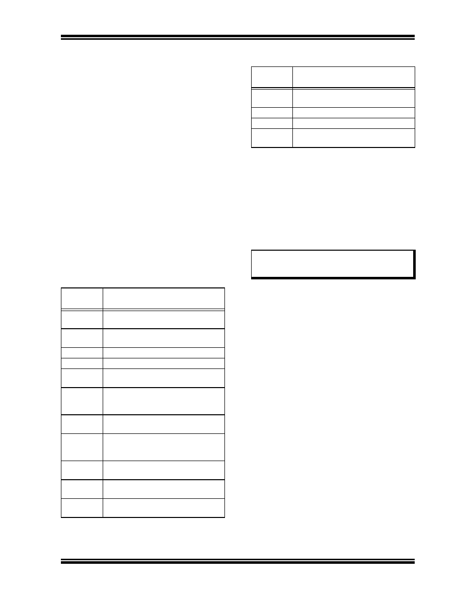
TABLE 11-2:
NVMCON ERASE
OPERATIONS
NVMCON
Value
Erase Operation
0x407F
Erase all code memory, data memory
(does not erase UNIT ID).
0x4075
Erase 1 row (16 words) of data
EEPROM.
0x4074
Erase 1 word of data EEPROM.
0x4072
Erase all executive memory.
0x4071
Erase 1 row (32 instruction words)
from 1 panel of code memory.
0x406E
Erase Boot Secure and General
Segments, then erase FBS, FSS and
FGS configuration registers.
0x4066
Erase all Data EEPROM allocated to
Boot Segment.
0x405E
Erase Secure and General Segments,
then erase FSS and FGS configuration
registers.
0x4056
Erase all Data EEPROM allocated to
Secure Segment.
0x404E
Erase General Segment, then erase
FGS configuration register.
0x4046
Erase all Data EEPROM allocated to
General Segment.
TABLE 11-3:
NVMCON WRITE
OPERATIONS
NVMCON
Value
Write Operation
0x4008
Write 1 word to configuration
memory.
0x4005
Write 1 row (16 words) to data memory.
0x4004
Write 1 word to data memory.
0x4001
Write 1 row (32 instruction words) into
1 panel of program memory.
11.4.2
UNLOCKING NVMCON FOR
PROGRAMMING
Writes to the WR bit (NVMCON<15>) are locked to
prevent accidental programming from taking place.
Writing a key sequence to the NVMKEY register
unlocks the WR bit and allows it to be written to. The
unlock sequence is performed as follows:
MOV
#0x55, W8
MOV
W8, NVMKEY
MOV
#0xAA, W9
MOV
W9, NVMKEY
Note:
Any working register, or working register
pair, can be used to write the unlock
sequence.
11.4.3
STARTING AND STOPPING A
PROGRAMMING CYCLE
Once the unlock key sequence has been written to the
NVMKEY register, the WR bit (NVMCON<15>) is used
to start and stop an erase or write cycle. Setting the WR
bit initiates the programming cycle. Clearing the WR bit
terminates the programming cycle.
All erase and write cycles must be externally timed. An
external delay must be used between setting and
clearing the WR bit. Starting and stopping a
programming cycle is performed as follows:
BSET
NVMCON, #WR
<Wait 2 ms>
BCLR
NVMCON, #WR
11.5
Erasing Program Memory in
Normal-Voltage Systems
The procedure for erasing program memory (all code
memory, data memory, executive memory and code-
protect bits) consists of setting NVMCON to 0x407F,
unlocking NVMCON for erasing and then executing the
programming cycle. This method of bulk erasing pro-
gram memory only works for systems where VDD is
between 4.5 volts and 5.5 volts. The method for erasing
program memory for systems with a lower VDD (3.0
volts-4.5 volts) is described in Section 6.1 “Erasing
相关PDF资料 |
PDF描述 |
|---|---|
| VI-271-IY-S | CONVERTER MOD DC/DC 12V 50W |
| MC14551BCPG | IC MUX/DEMUX QUAD 2X1 16DIP |
| VI-25K-IY-S | CONVERTER MOD DC/DC 40V 50W |
| ISL84544CPZ | IC SWITCH SPDT 8DIP |
| VI-25J-IY-S | CONVERTER MOD DC/DC 36V 50W |
相关代理商/技术参数 |
参数描述 |
|---|---|
| dsPIC30F4012-20I/ML | 功能描述:数字信号处理器和控制器 - DSP, DSC 44LD 20MIPS 48 KB RoHS:否 制造商:Microchip Technology 核心:dsPIC 数据总线宽度:16 bit 程序存储器大小:16 KB 数据 RAM 大小:2 KB 最大时钟频率:40 MHz 可编程输入/输出端数量:35 定时器数量:3 设备每秒兆指令数:50 MIPs 工作电源电压:3.3 V 最大工作温度:+ 85 C 封装 / 箱体:TQFP-44 安装风格:SMD/SMT |
| DSPIC30F4012-20I/SO | 功能描述:数字信号处理器和控制器 - DSP, DSC 16 Bit MCU/DSP 28LD 20M 48KB FL RoHS:否 制造商:Microchip Technology 核心:dsPIC 数据总线宽度:16 bit 程序存储器大小:16 KB 数据 RAM 大小:2 KB 最大时钟频率:40 MHz 可编程输入/输出端数量:35 定时器数量:3 设备每秒兆指令数:50 MIPs 工作电源电压:3.3 V 最大工作温度:+ 85 C 封装 / 箱体:TQFP-44 安装风格:SMD/SMT |
| DSPIC30F4012-20I/SP | 功能描述:数字信号处理器和控制器 - DSP, DSC 16 Bit MCU/DSP 28LD 20M 48KB FL RoHS:否 制造商:Microchip Technology 核心:dsPIC 数据总线宽度:16 bit 程序存储器大小:16 KB 数据 RAM 大小:2 KB 最大时钟频率:40 MHz 可编程输入/输出端数量:35 定时器数量:3 设备每秒兆指令数:50 MIPs 工作电源电压:3.3 V 最大工作温度:+ 85 C 封装 / 箱体:TQFP-44 安装风格:SMD/SMT |
| DSPIC30F4012-20I/SP | 制造商:Microchip Technology Inc 功能描述:16BIT MCU-DSP 20MHZ 30F4012 SDIL |
| DSPIC30F4012-30I/ML | 功能描述:数字信号处理器和控制器 - DSP, DSC Motor Control RoHS:否 制造商:Microchip Technology 核心:dsPIC 数据总线宽度:16 bit 程序存储器大小:16 KB 数据 RAM 大小:2 KB 最大时钟频率:40 MHz 可编程输入/输出端数量:35 定时器数量:3 设备每秒兆指令数:50 MIPs 工作电源电压:3.3 V 最大工作温度:+ 85 C 封装 / 箱体:TQFP-44 安装风格:SMD/SMT |
发布紧急采购,3分钟左右您将得到回复。