- 您现在的位置:买卖IC网 > PDF目录11342 > DSPIC30F4012-20E/ML (Microchip Technology)IC DSPIC MCU/DSP 48K 44QFN PDF资料下载
参数资料
| 型号: | DSPIC30F4012-20E/ML |
| 厂商: | Microchip Technology |
| 文件页数: | 32/66页 |
| 文件大小: | 0K |
| 描述: | IC DSPIC MCU/DSP 48K 44QFN |
| 产品培训模块: | Asynchronous Stimulus |
| 标准包装: | 45 |
| 系列: | dsPIC™ 30F |
| 核心处理器: | dsPIC |
| 芯体尺寸: | 16-位 |
| 速度: | 20 MIPS |
| 连通性: | CAN,I²C,SPI,UART/USART |
| 外围设备: | 高级欠压探测/复位,电机控制 PWM,QEI,POR,PWM,WDT |
| 输入/输出数: | 20 |
| 程序存储器容量: | 48KB(16K x 24) |
| 程序存储器类型: | 闪存 |
| EEPROM 大小: | 1K x 8 |
| RAM 容量: | 2K x 8 |
| 电压 - 电源 (Vcc/Vdd): | 2.5 V ~ 5.5 V |
| 数据转换器: | A/D 6x10b |
| 振荡器型: | 内部 |
| 工作温度: | -40°C ~ 125°C |
| 封装/外壳: | 44-VQFN 裸露焊盘 |
| 包装: | 管件 |
| 配用: | XLT44QFN4-ND - SOCKET TRANS ICE 28DIP TO 44QFN |
| 其它名称: | DSPIC30F401220EML |
第1页第2页第3页第4页第5页第6页第7页第8页第9页第10页第11页第12页第13页第14页第15页第16页第17页第18页第19页第20页第21页第22页第23页第24页第25页第26页第27页第28页第29页第30页第31页当前第32页第33页第34页第35页第36页第37页第38页第39页第40页第41页第42页第43页第44页第45页第46页第47页第48页第49页第50页第51页第52页第53页第54页第55页第56页第57页第58页第59页第60页第61页第62页第63页第64页第65页第66页
dsPIC30F Flash Programming Specification
DS70102K-page 38
2010 Microchip Technology Inc.
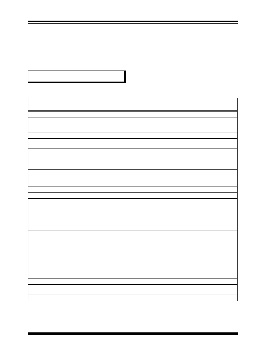
Table 11-4 shows the ICSP programming process for
bulk-erasing program memory. This process includes
the ICSP command code, which must be transmitted
(for each instruction) to the Least Significant bit first
using the PGC and PGD pins (see Figure 11-2).
If an individual Segment Erase operation is required,
the NVMCON value must be replaced by the value for
Note:
Program memory must be erased before
writing any data to program memory.
the corresponding Segment Erase operation.
TABLE 11-4:
SERIAL INSTRUCTION EXECUTION FOR BULK ERASING PROGRAM MEMORY
(ONLY IN NORMAL-VOLTAGE SYSTEMS)
Command
(Binary)
Data
(Hexadecimal)
Description
Step 1: Exit the Reset vector.
0000
040100
000000
GOTO 0x100
NOP
Step 2: Set NVMCON to program the FBS Configuration register.(1)
0000
24008A
883B0A
MOV
#0x4008, W10
MOV
W10, NVMCON
Step 3: Initialize the TBLPAG and write pointer (W7) for TBLWT instruction for Configuration register.(1)
0000
200F80
880190
200067
MOV
#0xF8, W0
MOV
W0, TBLPAG
MOV
#0x6, W7
Step 4: Load the Configuration Register data to W6.(1)
0000
EB0300
000000
CLR
W6
NOP
Step 5: Load the Configuration Register write latch. Advance W7 to point to next Configuration register.(1)
0000
BB1B86
TBLWTL W6, [W7++]
Step 6: Unlock the NVMCON for programming the Configuration register.(1)
0000
200558
200AA9
883B38
883B39
MOV
#0x55, W8
MOV
#0xAA, W9
MOV
W8, NVMKEY
MOV
W9, NVMKEY
Step 7: Initiate the programming cycle.(1)
0000
—
0000
A8E761
000000
—
000000
A9E761
000000
BSET NVMCON, #WR
NOP
Externally time 2 ms
NOP
BCLR NVMCON, #WR
NOP
Step 8: Repeat steps 5-7 one time to program 0x0000 to RESERVED2 Configuration register.(1)
Step 9: Set the NVMCON to erase all Program Memory.
00000
0000
2407FA
883B0A
MOV
#0x407F, W10
MOV
W10, NVMCON
Step 10: Unlock the NVMCON for programming.
Note 1: Steps 2-8 are only required for the dsPIC30F5011/5013 devices. These steps may be skipped for all other
devices in the dsPIC30F family.
相关PDF资料 |
PDF描述 |
|---|---|
| VI-271-IY-S | CONVERTER MOD DC/DC 12V 50W |
| MC14551BCPG | IC MUX/DEMUX QUAD 2X1 16DIP |
| VI-25K-IY-S | CONVERTER MOD DC/DC 40V 50W |
| ISL84544CPZ | IC SWITCH SPDT 8DIP |
| VI-25J-IY-S | CONVERTER MOD DC/DC 36V 50W |
相关代理商/技术参数 |
参数描述 |
|---|---|
| dsPIC30F4012-20I/ML | 功能描述:数字信号处理器和控制器 - DSP, DSC 44LD 20MIPS 48 KB RoHS:否 制造商:Microchip Technology 核心:dsPIC 数据总线宽度:16 bit 程序存储器大小:16 KB 数据 RAM 大小:2 KB 最大时钟频率:40 MHz 可编程输入/输出端数量:35 定时器数量:3 设备每秒兆指令数:50 MIPs 工作电源电压:3.3 V 最大工作温度:+ 85 C 封装 / 箱体:TQFP-44 安装风格:SMD/SMT |
| DSPIC30F4012-20I/SO | 功能描述:数字信号处理器和控制器 - DSP, DSC 16 Bit MCU/DSP 28LD 20M 48KB FL RoHS:否 制造商:Microchip Technology 核心:dsPIC 数据总线宽度:16 bit 程序存储器大小:16 KB 数据 RAM 大小:2 KB 最大时钟频率:40 MHz 可编程输入/输出端数量:35 定时器数量:3 设备每秒兆指令数:50 MIPs 工作电源电压:3.3 V 最大工作温度:+ 85 C 封装 / 箱体:TQFP-44 安装风格:SMD/SMT |
| DSPIC30F4012-20I/SP | 功能描述:数字信号处理器和控制器 - DSP, DSC 16 Bit MCU/DSP 28LD 20M 48KB FL RoHS:否 制造商:Microchip Technology 核心:dsPIC 数据总线宽度:16 bit 程序存储器大小:16 KB 数据 RAM 大小:2 KB 最大时钟频率:40 MHz 可编程输入/输出端数量:35 定时器数量:3 设备每秒兆指令数:50 MIPs 工作电源电压:3.3 V 最大工作温度:+ 85 C 封装 / 箱体:TQFP-44 安装风格:SMD/SMT |
| DSPIC30F4012-20I/SP | 制造商:Microchip Technology Inc 功能描述:16BIT MCU-DSP 20MHZ 30F4012 SDIL |
| DSPIC30F4012-30I/ML | 功能描述:数字信号处理器和控制器 - DSP, DSC Motor Control RoHS:否 制造商:Microchip Technology 核心:dsPIC 数据总线宽度:16 bit 程序存储器大小:16 KB 数据 RAM 大小:2 KB 最大时钟频率:40 MHz 可编程输入/输出端数量:35 定时器数量:3 设备每秒兆指令数:50 MIPs 工作电源电压:3.3 V 最大工作温度:+ 85 C 封装 / 箱体:TQFP-44 安装风格:SMD/SMT |
发布紧急采购,3分钟左右您将得到回复。