- 您现在的位置:买卖IC网 > PDF目录11256 > DSPIC30F5016-30I/PT (Microchip Technology)IC DSPIC MCU/DSP 66K 80TQFP PDF资料下载
参数资料
| 型号: | DSPIC30F5016-30I/PT |
| 厂商: | Microchip Technology |
| 文件页数: | 116/129页 |
| 文件大小: | 0K |
| 描述: | IC DSPIC MCU/DSP 66K 80TQFP |
| 产品培训模块: | dsPIC30F Quadrature Encoder Interface Serial Communications using dsPIC30F CAN Serial Communications using dsPIC30F I2C Serial Communications using dsPIC30F SPI Serial Communications using dsPIC30F UART dsPIC30F 12 bit ADC - Part 2 dsPIC30F Addressing Modes - Part 1 dsPIC30F Architecture - Part 1 dsPIC30F DSP Engine & ALU Asynchronous Stimulus dsPIC30F Addressing Modes - Part 2 dsPIC30F Architecture - Part 2 dsPIC30F 12-bit ADC Part 1 |
| 标准包装: | 119 |
| 系列: | dsPIC™ 30F |
| 核心处理器: | dsPIC |
| 芯体尺寸: | 16-位 |
| 速度: | 30 MIP |
| 连通性: | CAN,I²C,SPI,UART/USART |
| 外围设备: | 高级欠压探测/复位,电机控制 PWM,QEI,POR,PWM,WDT |
| 输入/输出数: | 68 |
| 程序存储器容量: | 66KB(22K x 24) |
| 程序存储器类型: | 闪存 |
| EEPROM 大小: | 1K x 8 |
| RAM 容量: | 2K x 8 |
| 电压 - 电源 (Vcc/Vdd): | 2.5 V ~ 5.5 V |
| 数据转换器: | A/D 16x10b |
| 振荡器型: | 内部 |
| 工作温度: | -40°C ~ 85°C |
| 封装/外壳: | 80-TQFP |
| 包装: | 托盘 |
| 产品目录页面: | 651 (CN2011-ZH PDF) |
| 配用: | AC164320-ND - MODULE SKT MPLAB PM3 80TQFP AC30F007-ND - MODULE SKT FOR DSPIC30F 80TQFP DV164005-ND - KIT ICD2 SIMPLE SUIT W/USB CABLE |
| 其它名称: | DSPIC30F501630IPT |
第1页第2页第3页第4页第5页第6页第7页第8页第9页第10页第11页第12页第13页第14页第15页第16页第17页第18页第19页第20页第21页第22页第23页第24页第25页第26页第27页第28页第29页第30页第31页第32页第33页第34页第35页第36页第37页第38页第39页第40页第41页第42页第43页第44页第45页第46页第47页第48页第49页第50页第51页第52页第53页第54页第55页第56页第57页第58页第59页第60页第61页第62页第63页第64页第65页第66页第67页第68页第69页第70页第71页第72页第73页第74页第75页第76页第77页第78页第79页第80页第81页第82页第83页第84页第85页第86页第87页第88页第89页第90页第91页第92页第93页第94页第95页第96页第97页第98页第99页第100页第101页第102页第103页第104页第105页第106页第107页第108页第109页第110页第111页第112页第113页第114页第115页当前第116页第117页第118页第119页第120页第121页第122页第123页第124页第125页第126页第127页第128页第129页
2008 Microchip Technology Inc.
DS70149D-page 87
dsPIC30F5015/5016
13.4.2
PWM PERIOD
The PWM period is specified by writing to the PRx
register. The PWM period can be calculated using
EQUATION 13-1:
PWM PERIOD
PWM frequency is defined as 1/[PWM period].
When the selected TMRx is equal to its respective
Period register, PRx, the following four events occur on
the next increment cycle:
TMRx is cleared.
The OCx pin is set.
- Exception 1: If PWM duty cycle is 0x0000,
the OCx pin will remain low.
- Exception 2: If duty cycle is greater than PRx,
the pin will remain high.
The PWM duty cycle is latched from OCxRS into
OCxR.
The corresponding timer interrupt flag is set.
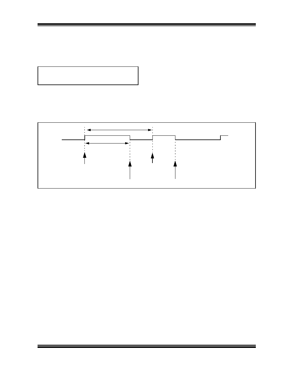
See Figure 13-1 for key PWM period comparisons.
Timer3 is referred to in the figure for clarity.
FIGURE 13-1:
PWM OUTPUT TIMING
13.5
Output Compare Operation During
CPU Sleep Mode
When the CPU enters the Sleep mode, all internal
clocks are stopped. Therefore, when the CPU enters
the Sleep state, the output compare channel will drive
the pin to the active state that was observed prior to
entering the CPU Sleep state.
For example, if the pin was high when the CPU
entered the Sleep state, the pin will remain high.
Likewise, if the pin was low when the CPU entered the
Sleep state, the pin will remain low. In either case, the
output compare module will resume operation when
the device wakes up.
13.6
Output Compare Operation During
CPU Idle Mode
When the CPU enters the Idle mode, the output
compare module can operate with full functionality.
The output compare channel will operate during the
CPU Idle mode if the OCSIDL bit (OCxCON<13>) is at
logic ‘0’ and the selected time base (Timer2 or Timer3)
is enabled and the TSIDL bit of the selected timer is
set to logic ‘0’.
13.7
Output Compare Interrupts
The output compare channels have the ability to
generate an interrupt on a compare match, for
whichever match mode has been selected.
For all modes except the PWM mode, when a compare
event occurs, the respective interrupt flag (OCxIF) is
asserted and an interrupt will be generated, if enabled.
The OCxIF bit is located in the corresponding IFS
Status register and must be cleared in software. The
interrupt is enabled via the respective Compare
Interrupt
Enable
(OCxIE)
bit,
located
in
the
corresponding IEC Control register.
For the PWM mode, when an event occurs, the
respective Timer Interrupt Flag (T2IF or T3IF) is
asserted and an interrupt will be generated, if enabled.
The IF bit is located in the IFS0 Status register and
must be cleared in software. The interrupt is enabled
via the respective Timer Interrupt Enable bit (T2IE or
T3IE), located in the IEC0 Control register. The output
compare interrupt flag is never set during the PWM
mode of operation.
PWM Period = [(PRx) + 1] 4 TOSC
(TMRx Prescale Value)
Period
Duty Cycle
TMR3 = Duty Cycle (OCxR)
TMR3 = PR3
T3IF = 1
(Interrupt Flag)
OCxR = OCxRS
TMR3 = PR3
(Interrupt Flag)
OCxR = OCxRS
T3IF = 1
相关PDF资料 |
PDF描述 |
|---|---|
| VI-J5R-IX-F3 | CONVERTER MOD DC/DC 7.5V 75W |
| ADG741BKSZ5-REEL7 | IC SWITCH SPST SC70-5 |
| ADG742BKSZ-REEL7 | IC SWITCH SPST SC70-6 |
| ADG3249BRJ-REEL7 | IC MUX/DEMUX 2X1 SOT23-8 |
| ADG742BKSZ5-REEL | IC SWITCH SPST SC70-5 |
相关代理商/技术参数 |
参数描述 |
|---|---|
| dsPIC30F5016T-20E/PT | 功能描述:数字信号处理器和控制器 - DSP, DSC 20MIPS 66 KB RoHS:否 制造商:Microchip Technology 核心:dsPIC 数据总线宽度:16 bit 程序存储器大小:16 KB 数据 RAM 大小:2 KB 最大时钟频率:40 MHz 可编程输入/输出端数量:35 定时器数量:3 设备每秒兆指令数:50 MIPs 工作电源电压:3.3 V 最大工作温度:+ 85 C 封装 / 箱体:TQFP-44 安装风格:SMD/SMT |
| DSPIC30F5016T-20I/PT | 功能描述:IC DSPIC MCU/DSP 66K 80TQFP RoHS:是 类别:集成电路 (IC) >> 嵌入式 - 微控制器, 系列:dsPIC™ 30F 产品培训模块:XLP Deep Sleep Mode 8-bit PIC® Microcontroller Portfolio 标准包装:22 系列:PIC® XLP™ 18F 核心处理器:PIC 芯体尺寸:8-位 速度:48MHz 连通性:I²C,SPI,UART/USART,USB 外围设备:欠压检测/复位,POR,PWM,WDT 输入/输出数:14 程序存储器容量:8KB(4K x 16) 程序存储器类型:闪存 EEPROM 大小:256 x 8 RAM 容量:512 x 8 电压 - 电源 (Vcc/Vdd):1.8 V ~ 5.5 V 数据转换器:A/D 11x10b 振荡器型:内部 工作温度:-40°C ~ 85°C 封装/外壳:20-DIP(0.300",7.62mm) 包装:管件 产品目录页面:642 (CN2011-ZH PDF) 配用:DV164126-ND - KIT DEVELOPMENT USB W/PICKIT 2DM164127-ND - KIT DEVELOPMENT USB 18F14/13K50AC164112-ND - VOLTAGE LIMITER MPLAB ICD2 VPP |
| dsPIC30F5016T-30I/PT | 功能描述:数字信号处理器和控制器 - DSP, DSC 30MIPS 66 KB RoHS:否 制造商:Microchip Technology 核心:dsPIC 数据总线宽度:16 bit 程序存储器大小:16 KB 数据 RAM 大小:2 KB 最大时钟频率:40 MHz 可编程输入/输出端数量:35 定时器数量:3 设备每秒兆指令数:50 MIPs 工作电源电压:3.3 V 最大工作温度:+ 85 C 封装 / 箱体:TQFP-44 安装风格:SMD/SMT |
| DSPIC30F6010-20E/PF | 功能描述:数字信号处理器和控制器 - DSP, DSC 30MHz 66KB Flash RoHS:否 制造商:Microchip Technology 核心:dsPIC 数据总线宽度:16 bit 程序存储器大小:16 KB 数据 RAM 大小:2 KB 最大时钟频率:40 MHz 可编程输入/输出端数量:35 定时器数量:3 设备每秒兆指令数:50 MIPs 工作电源电压:3.3 V 最大工作温度:+ 85 C 封装 / 箱体:TQFP-44 安装风格:SMD/SMT |
| DSPIC30F6010-20I/PF | 功能描述:数字信号处理器和控制器 - DSP, DSC 20MHz 144KB Flash RoHS:否 制造商:Microchip Technology 核心:dsPIC 数据总线宽度:16 bit 程序存储器大小:16 KB 数据 RAM 大小:2 KB 最大时钟频率:40 MHz 可编程输入/输出端数量:35 定时器数量:3 设备每秒兆指令数:50 MIPs 工作电源电压:3.3 V 最大工作温度:+ 85 C 封装 / 箱体:TQFP-44 安装风格:SMD/SMT |
发布紧急采购,3分钟左右您将得到回复。