- 您现在的位置:买卖IC网 > PDF目录3831 > DSPIC33FJ128GP202-I/SP (Microchip Technology)IC DSPIC MCU/DSP 128K 28DIP PDF资料下载
参数资料
| 型号: | DSPIC33FJ128GP202-I/SP |
| 厂商: | Microchip Technology |
| 文件页数: | 14/73页 |
| 文件大小: | 0K |
| 描述: | IC DSPIC MCU/DSP 128K 28DIP |
| 特色产品: | PIC24FJ/33FJ MCUs & dsPIC? DSCs |
| 标准包装: | 15 |
| 系列: | dsPIC™ 33F |
| 核心处理器: | dsPIC |
| 芯体尺寸: | 16-位 |
| 速度: | 40 MIP |
| 连通性: | I²C,IrDA,LIN,SPI,UART/USART |
| 外围设备: | AC'97,欠压检测/复位,DMA,I²S,POR,PWM,WDT |
| 输入/输出数: | 21 |
| 程序存储器容量: | 128KB(128K x 8) |
| 程序存储器类型: | 闪存 |
| RAM 容量: | 8K x 8 |
| 电压 - 电源 (Vcc/Vdd): | 3 V ~ 3.6 V |
| 数据转换器: | A/D 10x10b/12b |
| 振荡器型: | 内部 |
| 工作温度: | -40°C ~ 85°C |
| 封装/外壳: | 28-DIP(0.300",7.62mm) |
| 包装: | 管件 |
| 产品目录页面: | 653 (CN2011-ZH PDF) |
| 配用: | MA330019-ND - PIM DSPIC33F MC 44P-100P QFN DV164033-ND - KIT START EXPLORER 16 MPLAB ICD2 DV164005-ND - KIT ICD2 SIMPLE SUIT W/USB CABLE |
第1页第2页第3页第4页第5页第6页第7页第8页第9页第10页第11页第12页第13页当前第14页第15页第16页第17页第18页第19页第20页第21页第22页第23页第24页第25页第26页第27页第28页第29页第30页第31页第32页第33页第34页第35页第36页第37页第38页第39页第40页第41页第42页第43页第44页第45页第46页第47页第48页第49页第50页第51页第52页第53页第54页第55页第56页第57页第58页第59页第60页第61页第62页第63页第64页第65页第66页第67页第68页第69页第70页第71页第72页第73页
2007-2012 Microchip Technology Inc.
DS70292G-page 21
dsPIC33FJ32GP302/304, dsPIC33FJ64GPX02/X04, AND dsPIC33FJ128GPX02/X04
2.5
ICSP Pins
The PGECx and PGEDx pins are used for In-Circuit
Serial Programming (ICSP) and debugging pur-
poses. It is recommended to keep the trace length
between the ICSP connector and the ICSP pins on the
device as short as possible. If the ICSP connector is
expected to experience an ESD event, a series resistor
is recommended, with the value in the range of a few
tens of Ohms, not to exceed 100 Ohms.
Pull-up resistors, series diodes, and capacitors on the
PGECx and PGEDx pins are not recommended as they
will interfere with the programmer/debugger communi-
cations to the device. If such discrete components are
an application requirement, they should be removed
from the circuit during programming and debugging.
Alternatively, refer to the AC/DC characteristics and
timing requirements information in the respective
device Flash programming specification for information
on capacitive loading limits and pin input voltage high
(VIH) and input low (VIL) requirements.
Ensure that the “Communication Channel Select” (i.e.,
PGECx/PGEDx pins) programmed into the device
matches the physical connections for the ICSP to
MPLAB ICD 3 or MPLAB REAL ICE.
For more information on ICD 3 and REAL ICE
connection requirements, refer to the following
documents that are available on the Microchip website.
“Using MPLAB ICD 3 In-Circuit Debugger”
(poster) DS51765
“MPLAB ICD 3 Design Advisory” DS51764
“MPLAB REAL ICE In-Circuit Emulator User’s
Guide” DS51616
“Using MPLAB REAL ICE” (poster) DS51749
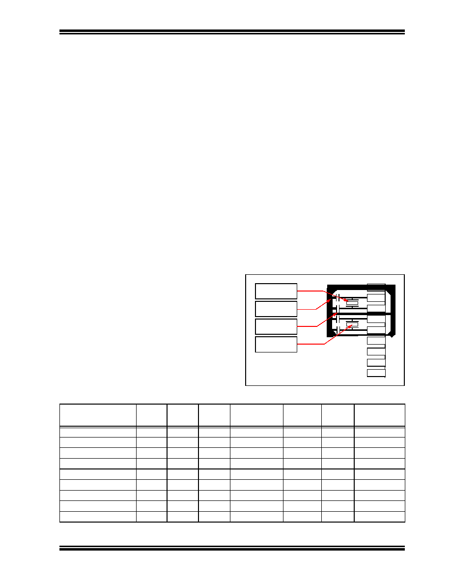
2.6
External Oscillator Pins
Many DSCs have options for at least two oscillators: a
high-frequency primary oscillator and a low-frequency
secondary oscillator (refer to Section 9.0 “Oscillator
Configuration” for details).
The oscillator circuit should be placed on the same
side of the board as the device. Also, place the
oscillator circuit close to the respective oscillator pins,
not exceeding one-half inch (12 mm) distance
between them. The load capacitors should be placed
next to the oscillator itself, on the same side of the
board. Use a grounded copper pour around the
oscillator circuit to isolate them from surrounding
circuits. The grounded copper pour should be routed
directly to the MCU ground. Do not run any signal
traces or power traces inside the ground pour. Also, if
using a two-sided board, avoid any traces on the
other side of the board where the crystal is placed. A
suggested
layout
is
shown
in
Recommendations
for
crystals
and
ceramic
resonators are provided in Table 2-1 and Table 2-2,
respectively.
FIGURE 2-3:
SUGGESTED PLACEMENT
OF THE OSCILLATOR
CIRCUIT
TABLE 2-1:
CRYSTAL RECOMMENDATIONS
13
Main Oscillator
Guard Ring
Guard Trace
Secondary
Oscillator
14
15
16
17
18
19
20
Part
Number
Vendor
Freq.
Load
Cap.
Package
Case
Frequency
Tolerance
Mounting
Type
Operating
Temperature
ECS-40-20-4DN
ECS Inc.
4 MHz
20 pF
HC49/US
±30 ppm
TH
-40°C to +85°C
ECS-80-18-4DN
ECS Inc.
8 MHz
18 pF
HC49/US
±30 ppm
TH
-40°C to +85°C
ECS-100-18-4-DN
ECS Inc.
10 MHz
18 pF
HC49/US
±30 ppm
TH
-40°C to +85°C
ECS-200-20-4DN
ECS Inc.
20 MHz
20 pF
HC49/US
±30 ppm
TH
-40°C to +85°C
ECS-40-20-5G3XDS-TR
ECS Inc.
4 MHz
20 pF
HC49/US
±30 ppm
SM
-40°C to +125°C
ECS-80-20-5G3XDS-TR
ECS Inc.
8 MHz
20 pF
HC49/US
±30 ppm
SM
-40°C to +125°C
ECS-100-20-5G3XDS-TR ECS Inc.
10 MHz
20 pF
HC49/US
±30 ppm
SM
-40°C to +125°C
ECS-200-20-5G3XDS-TR ECS Inc.
20 MHz
20 pF
HC49/US
±30 ppm
SM
-40°C to 125°C
NX3225SA 20MHZ AT-W NDK
20 MHz
8 pF
3.2 mm x 2.5 mm
±50 ppm
SM
-40°C to 125°C
Legend:
TH = Through Hole
SM = Surface Mount
相关PDF资料 |
PDF描述 |
|---|---|
| PIC24FJ128GA310-I/BG | MCU 16BIT 128KB FLASH 121TFBGA |
| PIC24HJ128GP204-I/PT | IC PIC MCU FLASH 128K 44TQFP |
| PIC18F8393-I/PT | IC PIC MCU FLASH 4KX16 80TQFP |
| DSPIC33FJ128GP204-I/PT | IC DSPIC MCU/DSP 128K 44TQFP |
| DSPIC33FJ64MC802-I/MM | IC DSPIC MCU/DSP 64K 28-QFN |
相关代理商/技术参数 |
参数描述 |
|---|---|
| dsPIC33FJ128GP202T-I/MM | 功能描述:数字信号处理器和控制器 - DSP, DSC 16B DSC 28LD128KB DMA 40MIPS RoHS:否 制造商:Microchip Technology 核心:dsPIC 数据总线宽度:16 bit 程序存储器大小:16 KB 数据 RAM 大小:2 KB 最大时钟频率:40 MHz 可编程输入/输出端数量:35 定时器数量:3 设备每秒兆指令数:50 MIPs 工作电源电压:3.3 V 最大工作温度:+ 85 C 封装 / 箱体:TQFP-44 安装风格:SMD/SMT |
| dsPIC33FJ128GP202T-I/SO | 功能描述:数字信号处理器和控制器 - DSP, DSC 16B DSC 28LD128KB DMA 40MIPS RoHS:否 制造商:Microchip Technology 核心:dsPIC 数据总线宽度:16 bit 程序存储器大小:16 KB 数据 RAM 大小:2 KB 最大时钟频率:40 MHz 可编程输入/输出端数量:35 定时器数量:3 设备每秒兆指令数:50 MIPs 工作电源电压:3.3 V 最大工作温度:+ 85 C 封装 / 箱体:TQFP-44 安装风格:SMD/SMT |
| dsPIC33FJ128GP204-E/ML | 功能描述:数字信号处理器和控制器 - DSP, DSC 16b DSC 128KB Flash DMA 40MIPS RoHS:否 制造商:Microchip Technology 核心:dsPIC 数据总线宽度:16 bit 程序存储器大小:16 KB 数据 RAM 大小:2 KB 最大时钟频率:40 MHz 可编程输入/输出端数量:35 定时器数量:3 设备每秒兆指令数:50 MIPs 工作电源电压:3.3 V 最大工作温度:+ 85 C 封装 / 箱体:TQFP-44 安装风格:SMD/SMT |
| dsPIC33FJ128GP204-E/PT | 功能描述:数字信号处理器和控制器 - DSP, DSC 16b DSC 128KB Flash DMA 40MIPS RoHS:否 制造商:Microchip Technology 核心:dsPIC 数据总线宽度:16 bit 程序存储器大小:16 KB 数据 RAM 大小:2 KB 最大时钟频率:40 MHz 可编程输入/输出端数量:35 定时器数量:3 设备每秒兆指令数:50 MIPs 工作电源电压:3.3 V 最大工作温度:+ 85 C 封装 / 箱体:TQFP-44 安装风格:SMD/SMT |
| dsPIC33FJ128GP204-I/ML | 功能描述:数字信号处理器和控制器 - DSP, DSC 16B DSC 44LD128KB DMA 40MIPS RoHS:否 制造商:Microchip Technology 核心:dsPIC 数据总线宽度:16 bit 程序存储器大小:16 KB 数据 RAM 大小:2 KB 最大时钟频率:40 MHz 可编程输入/输出端数量:35 定时器数量:3 设备每秒兆指令数:50 MIPs 工作电源电压:3.3 V 最大工作温度:+ 85 C 封装 / 箱体:TQFP-44 安装风格:SMD/SMT |
发布紧急采购,3分钟左右您将得到回复。