- 您现在的位置:买卖IC网 > PDF目录3831 > DSPIC33FJ128GP202-I/SP (Microchip Technology)IC DSPIC MCU/DSP 128K 28DIP PDF资料下载
参数资料
| 型号: | DSPIC33FJ128GP202-I/SP |
| 厂商: | Microchip Technology |
| 文件页数: | 60/73页 |
| 文件大小: | 0K |
| 描述: | IC DSPIC MCU/DSP 128K 28DIP |
| 特色产品: | PIC24FJ/33FJ MCUs & dsPIC? DSCs |
| 标准包装: | 15 |
| 系列: | dsPIC™ 33F |
| 核心处理器: | dsPIC |
| 芯体尺寸: | 16-位 |
| 速度: | 40 MIP |
| 连通性: | I²C,IrDA,LIN,SPI,UART/USART |
| 外围设备: | AC'97,欠压检测/复位,DMA,I²S,POR,PWM,WDT |
| 输入/输出数: | 21 |
| 程序存储器容量: | 128KB(128K x 8) |
| 程序存储器类型: | 闪存 |
| RAM 容量: | 8K x 8 |
| 电压 - 电源 (Vcc/Vdd): | 3 V ~ 3.6 V |
| 数据转换器: | A/D 10x10b/12b |
| 振荡器型: | 内部 |
| 工作温度: | -40°C ~ 85°C |
| 封装/外壳: | 28-DIP(0.300",7.62mm) |
| 包装: | 管件 |
| 产品目录页面: | 653 (CN2011-ZH PDF) |
| 配用: | MA330019-ND - PIM DSPIC33F MC 44P-100P QFN DV164033-ND - KIT START EXPLORER 16 MPLAB ICD2 DV164005-ND - KIT ICD2 SIMPLE SUIT W/USB CABLE |
第1页第2页第3页第4页第5页第6页第7页第8页第9页第10页第11页第12页第13页第14页第15页第16页第17页第18页第19页第20页第21页第22页第23页第24页第25页第26页第27页第28页第29页第30页第31页第32页第33页第34页第35页第36页第37页第38页第39页第40页第41页第42页第43页第44页第45页第46页第47页第48页第49页第50页第51页第52页第53页第54页第55页第56页第57页第58页第59页当前第60页第61页第62页第63页第64页第65页第66页第67页第68页第69页第70页第71页第72页第73页
2007-2012 Microchip Technology Inc.
DS70292G-page 63
dsPIC33FJ32GP302/304, dsPIC33FJ64GPX02/X04, AND dsPIC33FJ128GPX02/X04
4.6
Modulo Addressing
Modulo Addressing mode is a method of providing an
automated means to support circular data buffers using
hardware. The objective is to remove the need for
software to perform data address boundary checks
when executing tightly looped code, as is typical in
many DSP algorithms.
Modulo Addressing can operate in either data or program
space (since the data pointer mechanism is essentially
the same for both). One circular buffer can be supported
in each of the X (which also provides the pointers into
program space) and Y data spaces. Modulo Addressing
can operate on any W register pointer. However, it is not
advisable to use W14 or W15 for Modulo Addressing
since these two registers are used as the Stack Frame
Pointer and Stack Pointer, respectively.
In general, any particular circular buffer can be config-
ured to operate in only one direction as there are
certain restrictions on the buffer start address (for incre-
menting buffers), or end address (for decrementing
buffers), based upon the direction of the buffer.
The only exception to the usage restrictions is for
buffers that have a power-of-two length. As these
buffers satisfy the start and end address criteria, they
can operate in a bidirectional mode (that is, address
boundary checks are performed on both the lower and
upper address boundaries).
4.6.1
START AND END ADDRESS
The Modulo Addressing scheme requires that a
starting and ending address be specified and loaded
into the 16-bit Modulo Buffer Address registers:
XMODSRT, XMODEND, YMODSRT and YMODEND
(see Table 4-1).
The length of a circular buffer is not directly specified. It
is determined by the difference between the
corresponding start and end addresses. The maximum
possible length of the circular buffer is 32K words
(64 Kbytes).
4.6.2
W ADDRESS REGISTER
SELECTION
The Modulo and Bit-Reversed Addressing Control
register, MODCON<15:0>, contains enable flags as well
as a W register field to specify the W Address registers.
The XWM and YWM fields select the registers that
operate with Modulo Addressing:
If XWM = 15, X RAGU and X WAGU Modulo
Addressing is disabled.
If YWM = 15, Y AGU Modulo Addressing is
disabled.
The X Address Space Pointer W register (XWM), to
which Modulo Addressing is to be applied, is stored in
MODCON<3:0> (see Table 4-1). Modulo Addressing is
enabled for X data space when XWM is set to any value
other than ‘15’ and the XMODEN bit is set at
MODCON<15>.
The Y Address Space Pointer W register (YWM) to
which Modulo Addressing is to be applied is stored in
MODCON<7:4>. Modulo Addressing is enabled for Y
data space when YWM is set to any value other than
‘15’ and the YMODEN bit is set at MODCON<14>.
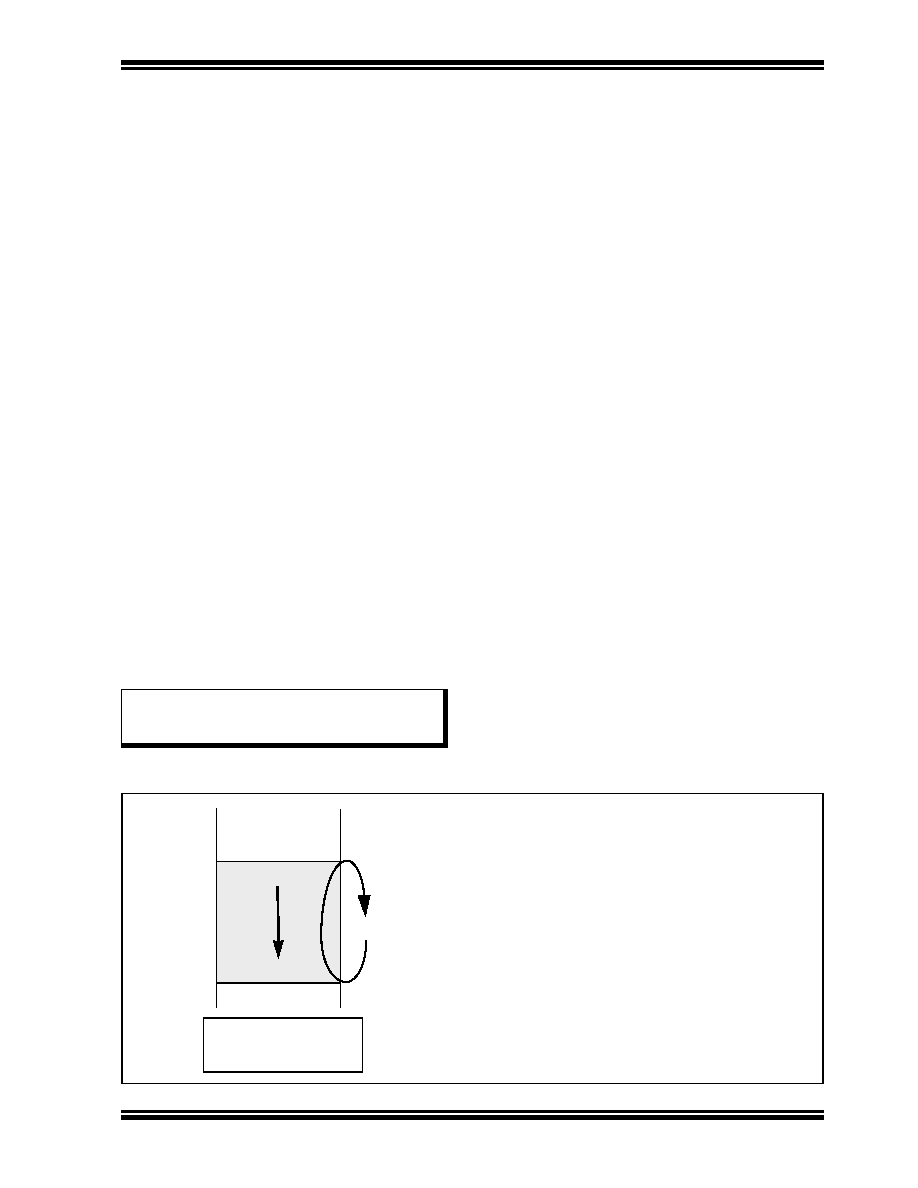
FIGURE 4-7:
MODULO ADDRESSING OPERATION EXAMPLE
Note:
Y
space
Modulo
Addressing
EA
calculations assume word-sized data (LSb
of every EA is always clear).
0x1100
0x1163
Start Addr = 0x1100
End Addr = 0x1163
Length = 0x0032 words
Byte
Address
MOV
#0x1100, W0
MOV
W0, XMODSRT
;set modulo start address
MOV
#0x1163, W0
MOV
W0, MODEND
;set modulo end address
MOV
#0x8001, W0
MOV
W0, MODCON
;enable W1, X AGU for modulo
MOV
#0x0000, W0
;W0 holds buffer fill value
MOV
#0x1110, W1
;point W1 to buffer
DO
AGAIN, #0x31
;fill the 50 buffer locations
MOV
W0, [W1++]
;fill the next location
AGAIN: INC W0, W0
;increment the fill value
相关PDF资料 |
PDF描述 |
|---|---|
| PIC24FJ128GA310-I/BG | MCU 16BIT 128KB FLASH 121TFBGA |
| PIC24HJ128GP204-I/PT | IC PIC MCU FLASH 128K 44TQFP |
| PIC18F8393-I/PT | IC PIC MCU FLASH 4KX16 80TQFP |
| DSPIC33FJ128GP204-I/PT | IC DSPIC MCU/DSP 128K 44TQFP |
| DSPIC33FJ64MC802-I/MM | IC DSPIC MCU/DSP 64K 28-QFN |
相关代理商/技术参数 |
参数描述 |
|---|---|
| dsPIC33FJ128GP202T-I/MM | 功能描述:数字信号处理器和控制器 - DSP, DSC 16B DSC 28LD128KB DMA 40MIPS RoHS:否 制造商:Microchip Technology 核心:dsPIC 数据总线宽度:16 bit 程序存储器大小:16 KB 数据 RAM 大小:2 KB 最大时钟频率:40 MHz 可编程输入/输出端数量:35 定时器数量:3 设备每秒兆指令数:50 MIPs 工作电源电压:3.3 V 最大工作温度:+ 85 C 封装 / 箱体:TQFP-44 安装风格:SMD/SMT |
| dsPIC33FJ128GP202T-I/SO | 功能描述:数字信号处理器和控制器 - DSP, DSC 16B DSC 28LD128KB DMA 40MIPS RoHS:否 制造商:Microchip Technology 核心:dsPIC 数据总线宽度:16 bit 程序存储器大小:16 KB 数据 RAM 大小:2 KB 最大时钟频率:40 MHz 可编程输入/输出端数量:35 定时器数量:3 设备每秒兆指令数:50 MIPs 工作电源电压:3.3 V 最大工作温度:+ 85 C 封装 / 箱体:TQFP-44 安装风格:SMD/SMT |
| dsPIC33FJ128GP204-E/ML | 功能描述:数字信号处理器和控制器 - DSP, DSC 16b DSC 128KB Flash DMA 40MIPS RoHS:否 制造商:Microchip Technology 核心:dsPIC 数据总线宽度:16 bit 程序存储器大小:16 KB 数据 RAM 大小:2 KB 最大时钟频率:40 MHz 可编程输入/输出端数量:35 定时器数量:3 设备每秒兆指令数:50 MIPs 工作电源电压:3.3 V 最大工作温度:+ 85 C 封装 / 箱体:TQFP-44 安装风格:SMD/SMT |
| dsPIC33FJ128GP204-E/PT | 功能描述:数字信号处理器和控制器 - DSP, DSC 16b DSC 128KB Flash DMA 40MIPS RoHS:否 制造商:Microchip Technology 核心:dsPIC 数据总线宽度:16 bit 程序存储器大小:16 KB 数据 RAM 大小:2 KB 最大时钟频率:40 MHz 可编程输入/输出端数量:35 定时器数量:3 设备每秒兆指令数:50 MIPs 工作电源电压:3.3 V 最大工作温度:+ 85 C 封装 / 箱体:TQFP-44 安装风格:SMD/SMT |
| dsPIC33FJ128GP204-I/ML | 功能描述:数字信号处理器和控制器 - DSP, DSC 16B DSC 44LD128KB DMA 40MIPS RoHS:否 制造商:Microchip Technology 核心:dsPIC 数据总线宽度:16 bit 程序存储器大小:16 KB 数据 RAM 大小:2 KB 最大时钟频率:40 MHz 可编程输入/输出端数量:35 定时器数量:3 设备每秒兆指令数:50 MIPs 工作电源电压:3.3 V 最大工作温度:+ 85 C 封装 / 箱体:TQFP-44 安装风格:SMD/SMT |
发布紧急采购,3分钟左右您将得到回复。