- 您现在的位置:买卖IC网 > PDF目录299030 > EP20K100BC324-1 (ALTERA CORP) LOADABLE PLD, PBGA324 PDF资料下载
参数资料
| 型号: | EP20K100BC324-1 |
| 厂商: | ALTERA CORP |
| 元件分类: | PLD |
| 英文描述: | LOADABLE PLD, PBGA324 |
| 文件页数: | 61/68页 |
| 文件大小: | 975K |
| 代理商: | EP20K100BC324-1 |
第1页第2页第3页第4页第5页第6页第7页第8页第9页第10页第11页第12页第13页第14页第15页第16页第17页第18页第19页第20页第21页第22页第23页第24页第25页第26页第27页第28页第29页第30页第31页第32页第33页第34页第35页第36页第37页第38页第39页第40页第41页第42页第43页第44页第45页第46页第47页第48页第49页第50页第51页第52页第53页第54页第55页第56页第57页第58页第59页第60页当前第61页第62页第63页第64页第65页第66页第67页第68页
64
4317K–AVR–03/2013
AT90PWM2/3/2B/3B
11.2.2
Toggling the Pin
Writing a logic one to PINxn toggles the value of PORTxn, independent on the value of DDRxn.
Note that the SBI instruction can be used to toggle one single bit in a port.
11.2.3
Switching Between Input and Output
When switching between tri-state ({DDxn, PORTxn} = 0b00) and output high ({DDxn, PORTxn}
= 0b11), an intermediate state with either pull-up enabled {DDxn, PORTxn} = 0b01) or output
low ({DDxn, PORTxn} = 0b10) must occur. Normally, the pull-up enabled state is fully accept-
able, as a high-impedant environment will not notice the difference between a strong high driver
and a pull-up. If this is not the case, the PUD bit in the MCUCR Register can be set to disable all
pull-ups in all ports.
Switching between input with pull-up and output low generates the same problem. The user
must use either the tri-state ({DDxn, PORTxn} = 0b00) or the output high state ({DDxn, PORTxn}
= 0b11) as an intermediate step.
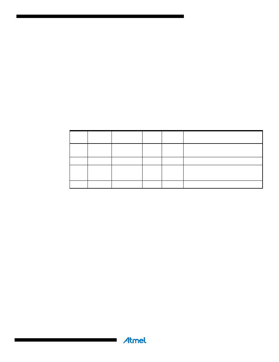
Table 11-1 summarizes the control signals for the pin value.
11.2.4
Reading the Pin Value
Independent of the setting of Data Direction bit DDxn, the port pin can be read through the
PINxn Register bit. As shown in Figure 11-2, the PINxn Register bit and the preceding latch con-
stitute a synchronizer. This is needed to avoid metastability if the physical pin changes value
near the edge of the internal clock, but it also introduces a delay. Figure 11-3 shows a timing dia-
gram of the synchronization when reading an externally applied pin value. The maximum and
minimum propagation delays are denoted t
pd,max and tpd,min respectively.
Table 11-1.
Port Pin Configurations
DDxn
PORTxn
PUD
(in MCUCR)
I/O
Pull-up
Comment
0
X
Input
No
Default configuration after Reset.
Tri-state (Hi-Z)
0
1
0
Input
Yes
Pxn will source current if ext. pulled low.
0
1
Input
No
Tri-state (Hi-Z)
1
0
X
Output
No
Output Low (Sink)
1
X
Output
No
Output High (Source)
相关PDF资料 |
PDF描述 |
|---|---|
| EP20K100BC324-2 | LOADABLE PLD, PBGA324 |
| EP20K100BC324-3 | LOADABLE PLD, PBGA324 |
| EP20K100BI324-1 | LOADABLE PLD, PBGA324 |
| EP20K100BI324-2 | LOADABLE PLD, PBGA324 |
| EP20K100BI324-3 | LOADABLE PLD, PBGA324 |
相关代理商/技术参数 |
参数描述 |
|---|---|
| EP20K100BC356-1 | 功能描述:FPGA - 现场可编程门阵列 CPLD - APEX 20K 416 Macro 252 IOs RoHS:否 制造商:Altera Corporation 系列:Cyclone V E 栅极数量: 逻辑块数量:943 内嵌式块RAM - EBR:1956 kbit 输入/输出端数量:128 最大工作频率:800 MHz 工作电源电压:1.1 V 最大工作温度:+ 70 C 安装风格:SMD/SMT 封装 / 箱体:FBGA-256 |
| EP20K100BC356-1ES | 制造商:未知厂家 制造商全称:未知厂家 功能描述:FPGA |
| EP20K100BC356-1V | 制造商:Rochester Electronics LLC 功能描述:- Bulk |
| EP20K100BC356-2 | 功能描述:FPGA - 现场可编程门阵列 CPLD - APEX 20K 416 Macro 252 IOs RoHS:否 制造商:Altera Corporation 系列:Cyclone V E 栅极数量: 逻辑块数量:943 内嵌式块RAM - EBR:1956 kbit 输入/输出端数量:128 最大工作频率:800 MHz 工作电源电压:1.1 V 最大工作温度:+ 70 C 安装风格:SMD/SMT 封装 / 箱体:FBGA-256 |
| EP20K100BC356-2ES | 制造商:未知厂家 制造商全称:未知厂家 功能描述:FPGA |
发布紧急采购,3分钟左右您将得到回复。