- 您现在的位置:买卖IC网 > PDF目录97915 > EP20K100ERC208-1ES Digitally Controlled Potentiometer (XDCP™) Terminal Voltage ±2.7V or ±5V, 128 Taps I2C Serial Interface; Temperature Range: -40°C to 85°C; Package: 10-MSOP PDF资料下载
参数资料
| 型号: | EP20K100ERC208-1ES |
| 元件分类: | 数字电位计 |
| 英文描述: | Digitally Controlled Potentiometer (XDCP™) Terminal Voltage ±2.7V or ±5V, 128 Taps I2C Serial Interface; Temperature Range: -40°C to 85°C; Package: 10-MSOP |
| 中文描述: | FPGA的 |
| 文件页数: | 88/114页 |
| 文件大小: | 1623K |
| 代理商: | EP20K100ERC208-1ES |
第1页第2页第3页第4页第5页第6页第7页第8页第9页第10页第11页第12页第13页第14页第15页第16页第17页第18页第19页第20页第21页第22页第23页第24页第25页第26页第27页第28页第29页第30页第31页第32页第33页第34页第35页第36页第37页第38页第39页第40页第41页第42页第43页第44页第45页第46页第47页第48页第49页第50页第51页第52页第53页第54页第55页第56页第57页第58页第59页第60页第61页第62页第63页第64页第65页第66页第67页第68页第69页第70页第71页第72页第73页第74页第75页第76页第77页第78页第79页第80页第81页第82页第83页第84页第85页第86页第87页当前第88页第89页第90页第91页第92页第93页第94页第95页第96页第97页第98页第99页第100页第101页第102页第103页第104页第105页第106页第107页第108页第109页第110页第111页第112页第113页第114页
Altera Corporation
75
APEX 20K Programmable Logic Device Family Data Sheet
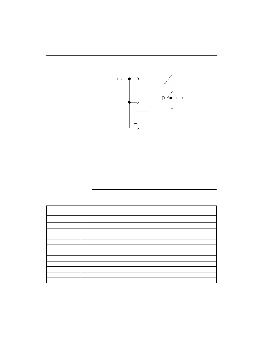
Figure 40. Synchronous Bidirectional Pin External Timing
Notes:
(1)
The output enable and input registers are LE registers in the LAB adjacent to a bi-
directional row pin. The output enable register is set with “Output Enable Routing=
Signal-Pin” option in the Quartus II software.
(2)
The LAB adjacent input register is set with “Decrease Input Delay to Internal Cells=
Off”. This maintains a zero hold time for lab adjacent registers while giving a fast,
position independent setup time. A faster setup time with zero hold time is possible
by setting “Decrease Input Delay to Internal Cells= ON” and moving the input
register farther away from the bi-directional pin. The exact position where zero
hold occurs with the minimum setup time, varies with device density and speed
grade.
PRN
CLRN
DQ
PRN
CLRN
DQ
(1)
IOE Register
Bidirectional Pin
Dedicated
Clock
PRN
CLRN
DQ
(1)
XZBIDIR
t
ZXBIDIR
t
OUTCOBIDIR
t
INSUBIDIR
t
INHBIDIR
t
OE Register
Output IOE Register
Input Register
(2)
Table 35. APEX 20K fMAX Timing Parameters
(Part 1 of 2)
Symbol
Parameter
tSU
LE register setup time before clock
tH
LE register hold time after clock
tCO
LE register clock-to-output delay
tLUT
LUT delay for data-in
tESBRC
ESB Asynchronous read cycle time
tESBWC
ESB Asynchronous write cycle time
tESBWESU
ESB WE setup time before clock when using input register
tESBDATASU
ESB data setup time before clock when using input register
tESBADDRSU
ESB address setup time before clock when using input registers
tESBDATACO1
ESB clock-to-output delay when using output registers
tESBDATACO2
ESB clock-to-output delay without output registers
相关PDF资料 |
PDF描述 |
|---|---|
| EP20K100ERC208-2ES | Digitally Controlled Potentiometer (XDCP™) Terminal Voltage ±2.7V or ±5V, 128 Taps I2C Serial Interface; Temperature Range: -40°C to 85°C; Package: 10-MSOP T&R |
| EP20K100ERC208-3ES | Single Digitally Controlled Potentiometer (XDCP™); Temperature Range: -40°C to 85°C; Package: 8-DFN |
| EP20K100ETI144-2ES | 600kHz/1.2MHz PWM Step-Up Regulator; Temperature Range: -40°C to 85°C; Package: 8-MSOP T&R |
| EP20K100ETI144-3ES | FPGA |
| EP20K100FC324-1 | Field Programmable Gate Array (FPGA) |
相关代理商/技术参数 |
参数描述 |
|---|---|
| EP20K100ERC208-2ES | 制造商:未知厂家 制造商全称:未知厂家 功能描述:FPGA |
| EP20K100ERC208-3ES | 制造商:未知厂家 制造商全称:未知厂家 功能描述:FPGA |
| EP20K100ERC240-1ES | 制造商:未知厂家 制造商全称:未知厂家 功能描述:FPGA |
| EP20K100ERC240-2ES | 制造商:未知厂家 制造商全称:未知厂家 功能描述:FPGA |
| EP20K100ERC240-3ES | 制造商:未知厂家 制造商全称:未知厂家 功能描述:FPGA |
发布紧急采购,3分钟左右您将得到回复。