- 您现在的位置:买卖IC网 > PDF目录97925 > EP20K400FI672-3 Field Programmable Gate Array (FPGA) PDF资料下载
参数资料
| 型号: | EP20K400FI672-3 |
| 英文描述: | Field Programmable Gate Array (FPGA) |
| 中文描述: | 现场可编程门阵列(FPGA) |
| 文件页数: | 63/114页 |
| 文件大小: | 1623K |
| 代理商: | EP20K400FI672-3 |
第1页第2页第3页第4页第5页第6页第7页第8页第9页第10页第11页第12页第13页第14页第15页第16页第17页第18页第19页第20页第21页第22页第23页第24页第25页第26页第27页第28页第29页第30页第31页第32页第33页第34页第35页第36页第37页第38页第39页第40页第41页第42页第43页第44页第45页第46页第47页第48页第49页第50页第51页第52页第53页第54页第55页第56页第57页第58页第59页第60页第61页第62页当前第63页第64页第65页第66页第67页第68页第69页第70页第71页第72页第73页第74页第75页第76页第77页第78页第79页第80页第81页第82页第83页第84页第85页第86页第87页第88页第89页第90页第91页第92页第93页第94页第95页第96页第97页第98页第99页第100页第101页第102页第103页第104页第105页第106页第107页第108页第109页第110页第111页第112页第113页第114页
52
Altera Corporation
APEX 20K Programmable Logic Device Family Data Sheet
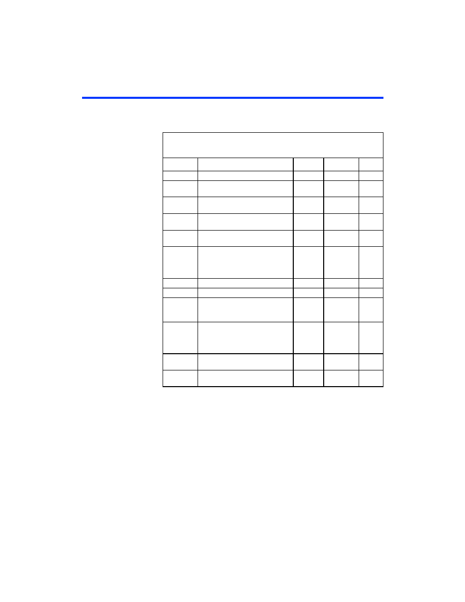
Table 16 summarizes the APEX 20K ClockLock and ClockBoost
parameters for -2 speed grade devices.
Notes:
(1)
To implement the ClockLock and ClockBoost circuitry with the Quartus II
software, designers must specify the input frequency. The Quartus II software
tunes the PLL in the ClockLock and ClockBoost circuitry to this frequency. The
fCLKDEV parameter specifies how much the incoming clock can differ from the
specified frequency during device operation. Simulation does not reflect this
parameter.
(2)
Twenty-five thousand parts per million (PPM) equates to 2.5% of input clock
period.
(3)
During device configuration, the ClockLock and ClockBoost circuitry is configured
before the rest of the device. If the incoming clock is supplied during configuration,
the ClockLock and ClockBoost circuitry locks during configuration because the
tLOCK value is less than the time required for configuration.
(4)
The tJITTER specification is measured under long-term observation.
Table 16. APEX 20K ClockLock & ClockBoost Parameters for -2 Speed Grade
Devices
Symbol
Parameter
Min
Max
Unit
fOUT
Output frequency
25
170
MHz
fCLK1
Input clock frequency (ClockBoost
clock multiplication factor equals 1)
25
170
MHz
fCLK2
Input clock frequency (ClockBoost
clock multiplication factor equals 2)
16
80
MHz
fCLK4
Input clock frequency (ClockBoost
clock multiplication factor equals 4)
10
34
MHz
tOUTDUTY
Duty cycle for ClockLock/ClockBoost-
generated clock
40
60
%
fCLKDEV
Input deviation from user specification
in the Quartus II software (ClockBoost
clock multiplication factor equals one)
25,000
PPM
tR
Input rise time
5ns
tF
Input fall time
5ns
tLOCK
Time required for ClockLock/
ClockBoost to acquire lock
10
s
tSKEW
Skew delay between related
ClockLock/ ClockBoost-generated
clock
500
ps
tJITTER
Jitter on ClockLock/ ClockBoost-
generated clock (4)
200
ps
tINCLKSTB
Input clock stability (measured between
adjacent clocks)
50
ps
相关PDF资料 |
PDF描述 |
|---|---|
| EP20K400FI672-3ES | FPGA |
| EP20K400GC655-1ES | FPGA |
| EP20K400GC655-2ES | RTC Module With CPU Supervisor |
| EP20K400GC655-3ES | RTC Module With CPU Supervisor |
| EP20K400GI655-1 | RTC Module With CPU Supervisor |
相关代理商/技术参数 |
参数描述 |
|---|---|
| EP20K400FI672-3ES | 制造商:未知厂家 制造商全称:未知厂家 功能描述:FPGA |
| EP20K400GC655-1ES | 制造商:未知厂家 制造商全称:未知厂家 功能描述:FPGA |
| EP20K400GC655-2 | 制造商:Rochester Electronics LLC 功能描述:- Bulk |
| EP20K400GC655-2ES | 制造商:未知厂家 制造商全称:未知厂家 功能描述:FPGA |
| EP20K400GC655-3 | 制造商:Rochester Electronics LLC 功能描述:- Bulk |
发布紧急采购,3分钟左右您将得到回复。