参数资料
| 型号: | EP2AGX190FF35C5N |
| 厂商: | Altera |
| 文件页数: | 3/90页 |
| 文件大小: | 0K |
| 描述: | IC ARRIA II GX 190K 1152FBGA |
| 产品培训模块: | Three Reasons to Use FPGA's in Industrial Designs |
| 标准包装: | 3 |
| 系列: | Arria II GX |
| LAB/CLB数: | 7612 |
| 逻辑元件/单元数: | 181165 |
| RAM 位总计: | 10177536 |
| 输入/输出数: | 612 |
| 电源电压: | 0.87 V ~ 0.93 V |
| 安装类型: | 表面贴装 |
| 工作温度: | 0°C ~ 85°C |
| 封装/外壳: | 1152-BBGA |
| 供应商设备封装: | 1152-FBGA(27x27) |
第1页第2页当前第3页第4页第5页第6页第7页第8页第9页第10页第11页第12页第13页第14页第15页第16页第17页第18页第19页第20页第21页第22页第23页第24页第25页第26页第27页第28页第29页第30页第31页第32页第33页第34页第35页第36页第37页第38页第39页第40页第41页第42页第43页第44页第45页第46页第47页第48页第49页第50页第51页第52页第53页第54页第55页第56页第57页第58页第59页第60页第61页第62页第63页第64页第65页第66页第67页第68页第69页第70页第71页第72页第73页第74页第75页第76页第77页第78页第79页第80页第81页第82页第83页第84页第85页第86页第87页第88页第89页第90页
Chapter 1: Device Datasheet for Arria II Devices
1–3
Electrical Characteristics
December 2013
Altera Corporation
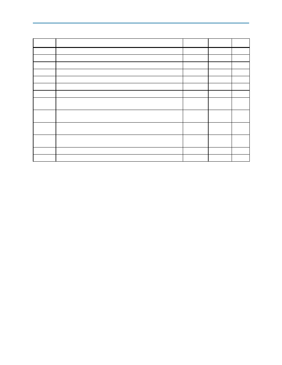
Maximum Allowed Overshoot and Undershoot Voltage
During transitions, input signals may overshoot to the voltage shown in Table 1–3 and
undershoot to –2.0 V for magnitude of currents less than 100 mA and periods shorter
than 20 ns.
Table 1–3 lists the Arria II GX and GZ maximum allowed input overshoot voltage and
the duration of the overshoot voltage as a percentage over the device lifetime. The
maximum allowed overshoot duration is specified as a percentage of high-time over
the lifetime of the device. A DC signal is equivalent to 100% duty cycle. For example,
a signal that overshoots to 4.3 V can only be at 4.3 V for 5.41% over the lifetime of the
device; for a device lifetime of 10 years, this amounts to 5.41/10ths of a year.
VCCA_L
Supplies transceiver high voltage power (left side)
-0.5
3.75
V
VCCA_R
Supplies transceiver high voltage power (right side)
-0.5
3.75
V
VCCHIP_L
Supplies transceiver HIP digital power (left side)
-0.5
1.35
V
VCCR_L
Supplies receiver power (left side)
-0.5
1.35
V
VCCR_R
Supplies receiver power (right side)
-0.5
1.35
V
VCCT_L
Supplies transmitter power (left side)
-0.5
1.35
V
VCCT_R
Supplies transmitter power (right side)
-0.5
1.35
V
VCCL_GXBLn
Supplies power to the transceiver PMA TX, PMA RX, and clocking (left
side)
-0.5
1.35
V
VCCL_GXBRn
Supplies power to the transceiver PMA TX, PMA RX, and clocking (right
side)
-0.5
1.35
V
VCCH_GXBLn
Supplies power to the transceiver PMA output (TX) buffer (left side)
-0.5
1.8
V
VCCH_GXBRn
Supplies power to the transceiver PMA output (TX) buffer (right side)
-0.5
1.8
V
TJ
Operating junction temperature
-55
125
°C
TSTG
Storage temperature (no bias)
-65
150
°C
Note to Table 1–2:
(1) n = 0, 1, or 2.
Table 1–2. Absolute Maximum Ratings for Arria II GZ Devices (Part 2 of 2)
Symbol
Description
Minimum
Maximum
Unit
相关PDF资料 |
PDF描述 |
|---|---|
| EP2AGX190EF29I5N | IC ARRIA II GX FPGA 190K 780FBGA |
| HSC44DRAH-S734 | CONN EDGECARD 88POS .100 R/A PCB |
| EP2AGX190EF29C4N | IC ARRIA II GX FPGA 190K 780FBGA |
| FMC22DRYN | CONN EDGECARD 44POS DIP .100 SLD |
| EP1S30F780I6 | IC STRATIX FPGA 30K LE 780-FBGA |
相关代理商/技术参数 |
参数描述 |
|---|---|
| EP2AGX190FF35C6 | 功能描述:FPGA - 现场可编程门阵列 FPGA - Arria II GX 7612 LABs 612 IOs RoHS:否 制造商:Altera Corporation 系列:Cyclone V E 栅极数量: 逻辑块数量:943 内嵌式块RAM - EBR:1956 kbit 输入/输出端数量:128 最大工作频率:800 MHz 工作电源电压:1.1 V 最大工作温度:+ 70 C 安装风格:SMD/SMT 封装 / 箱体:FBGA-256 |
| EP2AGX190FF35C6N | 功能描述:FPGA - 现场可编程门阵列 FPGA - Arria II GX 7612 LABs 612 IOs RoHS:否 制造商:Altera Corporation 系列:Cyclone V E 栅极数量: 逻辑块数量:943 内嵌式块RAM - EBR:1956 kbit 输入/输出端数量:128 最大工作频率:800 MHz 工作电源电压:1.1 V 最大工作温度:+ 70 C 安装风格:SMD/SMT 封装 / 箱体:FBGA-256 |
| EP2AGX190FF35C6NGA | 制造商:Altera 功能描述:EP2AGX190FF35C6NGA |
| EP2AGX190FF35I3 | 功能描述:IC ARRIA II GX 190K 1152FBGA RoHS:否 类别:集成电路 (IC) >> 嵌入式 - FPGA(现场可编程门阵列) 系列:Arria II GX 产品变化通告:XC4000(E,L) Discontinuation 01/April/2002 标准包装:24 系列:XC4000E/X LAB/CLB数:100 逻辑元件/单元数:238 RAM 位总计:3200 输入/输出数:80 门数:3000 电源电压:4.5 V ~ 5.5 V 安装类型:表面贴装 工作温度:-40°C ~ 100°C 封装/外壳:120-BCBGA 供应商设备封装:120-CPGA(34.55x34.55) |
| EP2AGX190FF35I3N | 功能描述:FPGA - 现场可编程门阵列 FPGA - Arria II GX 7612 LABs 612 IOs RoHS:否 制造商:Altera Corporation 系列:Cyclone V E 栅极数量: 逻辑块数量:943 内嵌式块RAM - EBR:1956 kbit 输入/输出端数量:128 最大工作频率:800 MHz 工作电源电压:1.1 V 最大工作温度:+ 70 C 安装风格:SMD/SMT 封装 / 箱体:FBGA-256 |
发布紧急采购,3分钟左右您将得到回复。