- 您现在的位置:买卖IC网 > PDF目录19912 > EPCS1SI8 (Altera)IC CONFIG DEVICE 1MBIT 8-SOIC PDF资料下载
参数资料
| 型号: | EPCS1SI8 |
| 厂商: | Altera |
| 文件页数: | 13/40页 |
| 文件大小: | 0K |
| 描述: | IC CONFIG DEVICE 1MBIT 8-SOIC |
| 产品培训模块: | Three Reasons to Use FPGA's in Industrial Designs |
| 标准包装: | 100 |
| 系列: | EPCS |
| 可编程类型: | 系统内可编程 |
| 存储容量: | 1Mb |
| 电源电压: | 3 V ~ 3.6 V |
| 工作温度: | -40°C ~ 85°C |
| 封装/外壳: | 8-SOIC(0.154",3.90mm 宽) |
| 供应商设备封装: | 8-SOIC |
| 包装: | 管件 |
| 产品目录页面: | 604 (CN2011-ZH PDF) |
| 其它名称: | 544-1241-5 |
第1页第2页第3页第4页第5页第6页第7页第8页第9页第10页第11页第12页当前第13页第14页第15页第16页第17页第18页第19页第20页第21页第22页第23页第24页第25页第26页第27页第28页第29页第30页第31页第32页第33页第34页第35页第36页第37页第38页第39页第40页
Page 20
EPCS Device Memory Access
Serial Configuration (EPCS) Devices Datasheet
January 2014
Altera Corporation
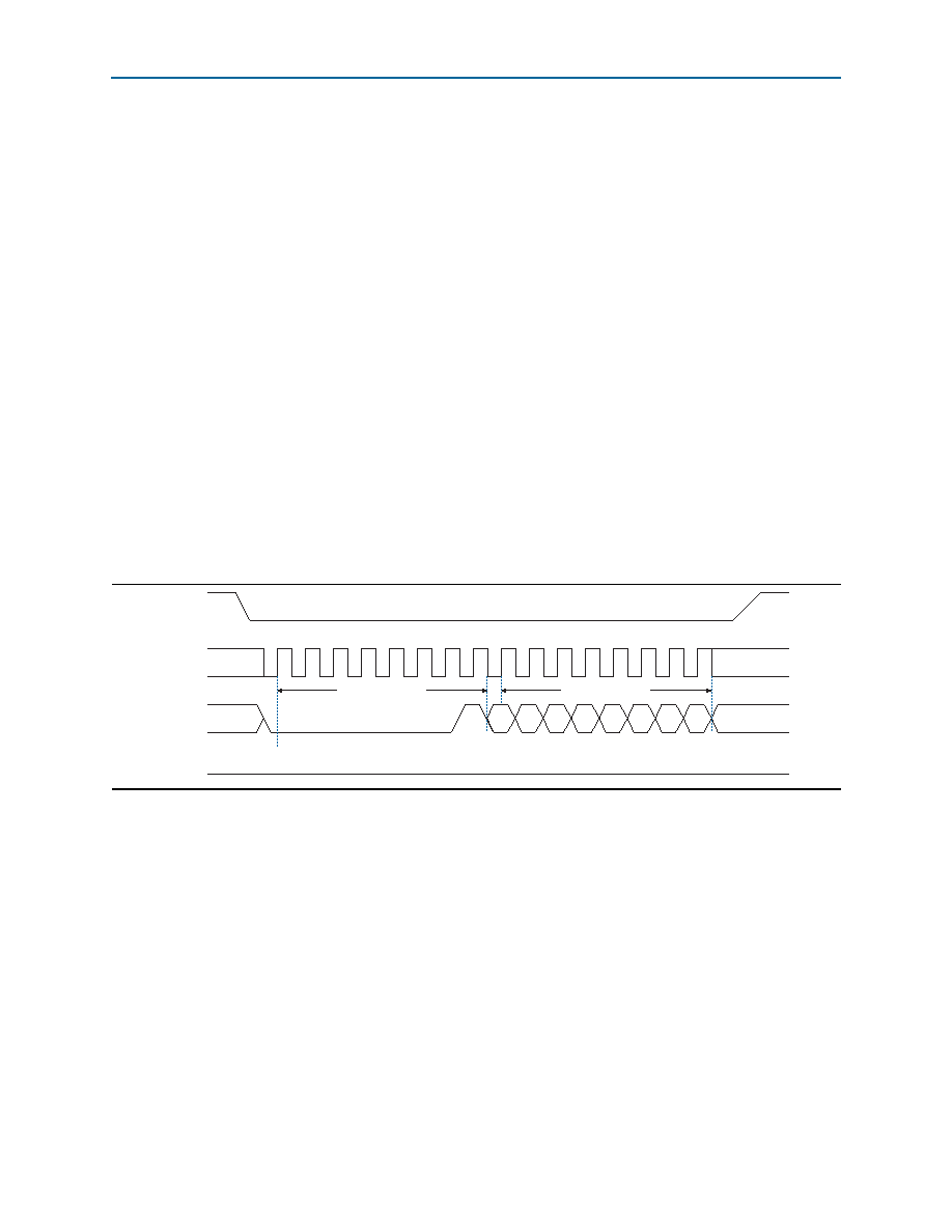
Write Status Operation
The write status operation code is b'0000 0001 and it lists the MSB first. Use the write
status operation to set the status register block protection bits. The write status
operation does not affect the other bits. Therefore, you can implement this operation
the block protect bits, the protected memory sectors are treated as read-only memory.
You must execute the write enable operation before the write status operation so the
device sets the status register’s write enable latch bit to 1.
The write status operation is implemented by driving the nCS signal low, followed by
shifting in the write status operation code and one data byte for the status register on
the ASDI pin. Figure 10 shows the instruction sequence of the write status operation.
The nCS must be driven high after the eighth bit of the data byte has been latched in,
otherwise the write status operation is not executed.
Immediately after the nCS signal drives high, the device initiates the self-timed write
status cycle. The self-timed write status cycle usually takes 5 ms for all EPCS devices
and is guaranteed to be less than 15 ms. For more information, refer to the tWS value in
Table 16 on page 29. You must account for this delay to ensure that the status register
is written with desired block protect bits. Alternatively, you can check the write in
progress bit in the status register by executing the read status operation while the
self-timed write status cycle is in progress. The write in progress bit is 1 during the
self-timed write status cycle and 0 when it is complete.
Read Bytes Operation
The read bytes operation code is b'0000 0011 and it lists the MSB first. To read the
memory contents of the EPCS device, the device is first selected by driving the nCS
signal low. Then, the read bytes operation code is shifted in followed by a 3-byte
address (A[23..0]). Each address bit must be latched in on the rising edge of the DCLK
signal. After the address is latched in, the memory contents of the specified address
are shifted out serially on the DATA pin, beginning with the MSB. For reading Raw
Programming Data files (.rpd), the content is shifted out serially beginning with the
LSB. Each data bit is shifted out on the falling edge of the DCLK signal. The maximum
DCLK
frequency during the read bytes operation is 20 MHz.
Figure 10. Write Status Operation Timing Diagram
nCS
DCLK
ASDI
DATA
0
1
2
3
4
5
6
7
8
9
101112131415
Operation Code
Status Register
76543210
MSB
High Impedance
相关PDF资料 |
PDF描述 |
|---|---|
| EBC10DREF-S13 | CONN EDGECARD 20POS .100 EXTEND |
| GRM2165C2A161JA01D | CAP CER 160PF 100V 5% NP0 0805 |
| RMC05DRYI | CONN EDGECARD 10POS DIP .100 SLD |
| ABB45DHRR | CONN CARD EXTEND 90POS .050" |
| TAS476K020P1F-F | CAP TANT 47UF 20V 10% AXIAL |
相关代理商/技术参数 |
参数描述 |
|---|---|
| EPCS1SI8N | 功能描述:FPGA-配置存储器 IC - Ser. Config Mem Flash 1Mb 40 MHz RoHS:否 制造商:Altera Corporation 存储类型:Flash 存储容量:1.6 Mbit 工作频率:10 MHz 电源电压-最大:5.25 V 电源电压-最小:3 V 电源电流:50 uA 最大工作温度:+ 85 C 最小工作温度:- 40 C 安装风格:SMD/SMT 封装 / 箱体:PLCC-20 |
| EPCS250 | 制造商:Electrolube 功能描述:COATING MASK PEELABLE 250 制造商:Electrolube 功能描述:COATING MASK, PEELABLE 250 |
| EPCS2PC1 | 制造商:Switchcraft 功能描述: |
| EPCS4 | 制造商:ALTERA 制造商全称:Altera Corporation 功能描述:Serial Configuration Devices |
| EPCS4SI8 | 功能描述:FPGA-配置存储器 IC - Ser. Config Mem Flash 4Mb 40 MHz RoHS:否 制造商:Altera Corporation 存储类型:Flash 存储容量:1.6 Mbit 工作频率:10 MHz 电源电压-最大:5.25 V 电源电压-最小:3 V 电源电流:50 uA 最大工作温度:+ 85 C 最小工作温度:- 40 C 安装风格:SMD/SMT 封装 / 箱体:PLCC-20 |
发布紧急采购,3分钟左右您将得到回复。