- 您现在的位置:买卖IC网 > PDF目录19912 > EPCS1SI8 (Altera)IC CONFIG DEVICE 1MBIT 8-SOIC PDF资料下载
参数资料
| 型号: | EPCS1SI8 |
| 厂商: | Altera |
| 文件页数: | 7/40页 |
| 文件大小: | 0K |
| 描述: | IC CONFIG DEVICE 1MBIT 8-SOIC |
| 产品培训模块: | Three Reasons to Use FPGA's in Industrial Designs |
| 标准包装: | 100 |
| 系列: | EPCS |
| 可编程类型: | 系统内可编程 |
| 存储容量: | 1Mb |
| 电源电压: | 3 V ~ 3.6 V |
| 工作温度: | -40°C ~ 85°C |
| 封装/外壳: | 8-SOIC(0.154",3.90mm 宽) |
| 供应商设备封装: | 8-SOIC |
| 包装: | 管件 |
| 产品目录页面: | 604 (CN2011-ZH PDF) |
| 其它名称: | 544-1241-5 |
第1页第2页第3页第4页第5页第6页当前第7页第8页第9页第10页第11页第12页第13页第14页第15页第16页第17页第18页第19页第20页第21页第22页第23页第24页第25页第26页第27页第28页第29页第30页第31页第32页第33页第34页第35页第36页第37页第38页第39页第40页
EPCS Device Memory Access
Page 15
Serial Configuration (EPCS) Devices Datasheet
January 2014
Altera Corporation
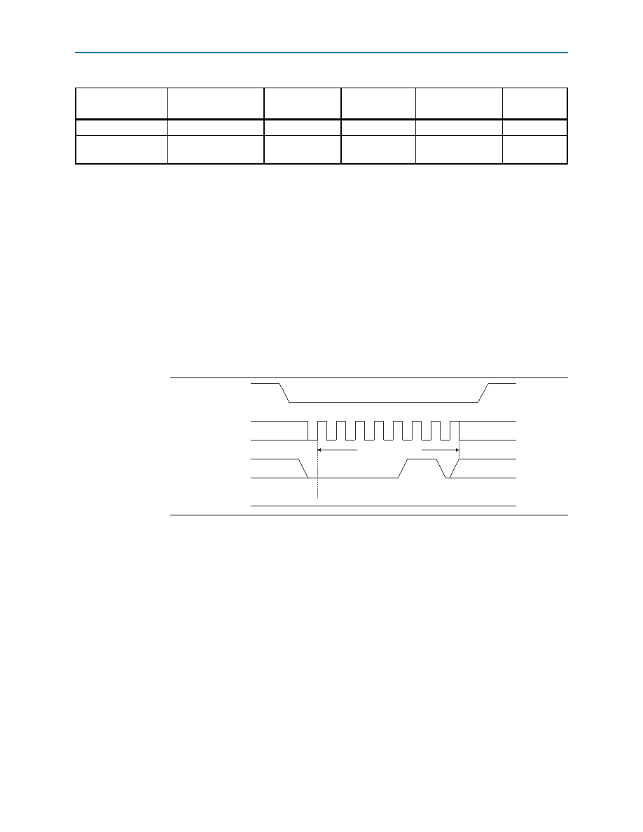
Write Enable Operation
The write enable operation code is b'0000 0110, and it lists the MSB first. The write
enable operation sets the write enable latch bit, which is bit 1 in the status register.
Always set the write enable latch bit before write bytes, write status, erase bulk, and
erase sector operations. Figure 5 shows the instruction sequence of the write enable
operation.
Write Disable Operation
The write disable operation code is b'0000 0100 and it lists the MSB first. The write
disable operation resets the write enable latch bit, which is bit 1 in the status register.
To prevent the memory from being written unintentionally, the write enable latch bit
is automatically reset when implementing the write disable operation, and under the
following conditions:
■
Power up
■
Write bytes operation completion
■
Write status operation completion
■
Erase bulk operation completion
■
Erase sector operation completion
Erase sector
1101 1000
30
0
25
Read device
identification (5)
1001 1111
0
2
1 to infinite (2)
25
Notes to Table 8:
(1) List MSB first and LSB last.
(2) The status register, data, or silicon ID is read out at least once on the DATA pin and is continuously read out until the nCS pin is driven high.
(3) A write bytes operation requires at least one data byte on the DATA pin. If more than 256 bytes are sent to the device, only the last 256 bytes
are written to the memory.
(4) The read silicon ID operation is available only for EPCS1, EPCS4, EPCS16, and EPCS64 devices.
(5) The read device identification operation is available only for EPCS128 devices.
Table 8. EPCS Devices Operation Codes
Operation
Operation Code (1)
Address Bytes
Dummy Bytes
Data Bytes
DCLK fMAX
(MHz)
Figure 5. Write Enable Operation Timing Diagram
nCS
DCLK
ASDI
DATA
01234567
Operation Code
High Impedance
相关PDF资料 |
PDF描述 |
|---|---|
| EBC10DREF-S13 | CONN EDGECARD 20POS .100 EXTEND |
| GRM2165C2A161JA01D | CAP CER 160PF 100V 5% NP0 0805 |
| RMC05DRYI | CONN EDGECARD 10POS DIP .100 SLD |
| ABB45DHRR | CONN CARD EXTEND 90POS .050" |
| TAS476K020P1F-F | CAP TANT 47UF 20V 10% AXIAL |
相关代理商/技术参数 |
参数描述 |
|---|---|
| EPCS1SI8N | 功能描述:FPGA-配置存储器 IC - Ser. Config Mem Flash 1Mb 40 MHz RoHS:否 制造商:Altera Corporation 存储类型:Flash 存储容量:1.6 Mbit 工作频率:10 MHz 电源电压-最大:5.25 V 电源电压-最小:3 V 电源电流:50 uA 最大工作温度:+ 85 C 最小工作温度:- 40 C 安装风格:SMD/SMT 封装 / 箱体:PLCC-20 |
| EPCS250 | 制造商:Electrolube 功能描述:COATING MASK PEELABLE 250 制造商:Electrolube 功能描述:COATING MASK, PEELABLE 250 |
| EPCS2PC1 | 制造商:Switchcraft 功能描述: |
| EPCS4 | 制造商:ALTERA 制造商全称:Altera Corporation 功能描述:Serial Configuration Devices |
| EPCS4SI8 | 功能描述:FPGA-配置存储器 IC - Ser. Config Mem Flash 4Mb 40 MHz RoHS:否 制造商:Altera Corporation 存储类型:Flash 存储容量:1.6 Mbit 工作频率:10 MHz 电源电压-最大:5.25 V 电源电压-最小:3 V 电源电流:50 uA 最大工作温度:+ 85 C 最小工作温度:- 40 C 安装风格:SMD/SMT 封装 / 箱体:PLCC-20 |
发布紧急采购,3分钟左右您将得到回复。