- 您现在的位置:买卖IC网 > PDF目录16601 > EVAL-AD5292EBZ (Analog Devices Inc)BOARD EVAL FOR AD5292 PDF资料下载
参数资料
| 型号: | EVAL-AD5292EBZ |
| 厂商: | Analog Devices Inc |
| 文件页数: | 21/32页 |
| 文件大小: | 0K |
| 描述: | BOARD EVAL FOR AD5292 |
| 标准包装: | 1 |
| 主要目的: | 数字电位器 |
| 嵌入式: | 是 |
| 已用 IC / 零件: | AD5292 |
| 主要属性: | 1 通道,1024 位置 |
| 次要属性: | SPI 接口 |
| 已供物品: | 板,CD |
第1页第2页第3页第4页第5页第6页第7页第8页第9页第10页第11页第12页第13页第14页第15页第16页第17页第18页第19页第20页当前第21页第22页第23页第24页第25页第26页第27页第28页第29页第30页第31页第32页
AD5291/AD5292
Rev. D | Page 28 of 32
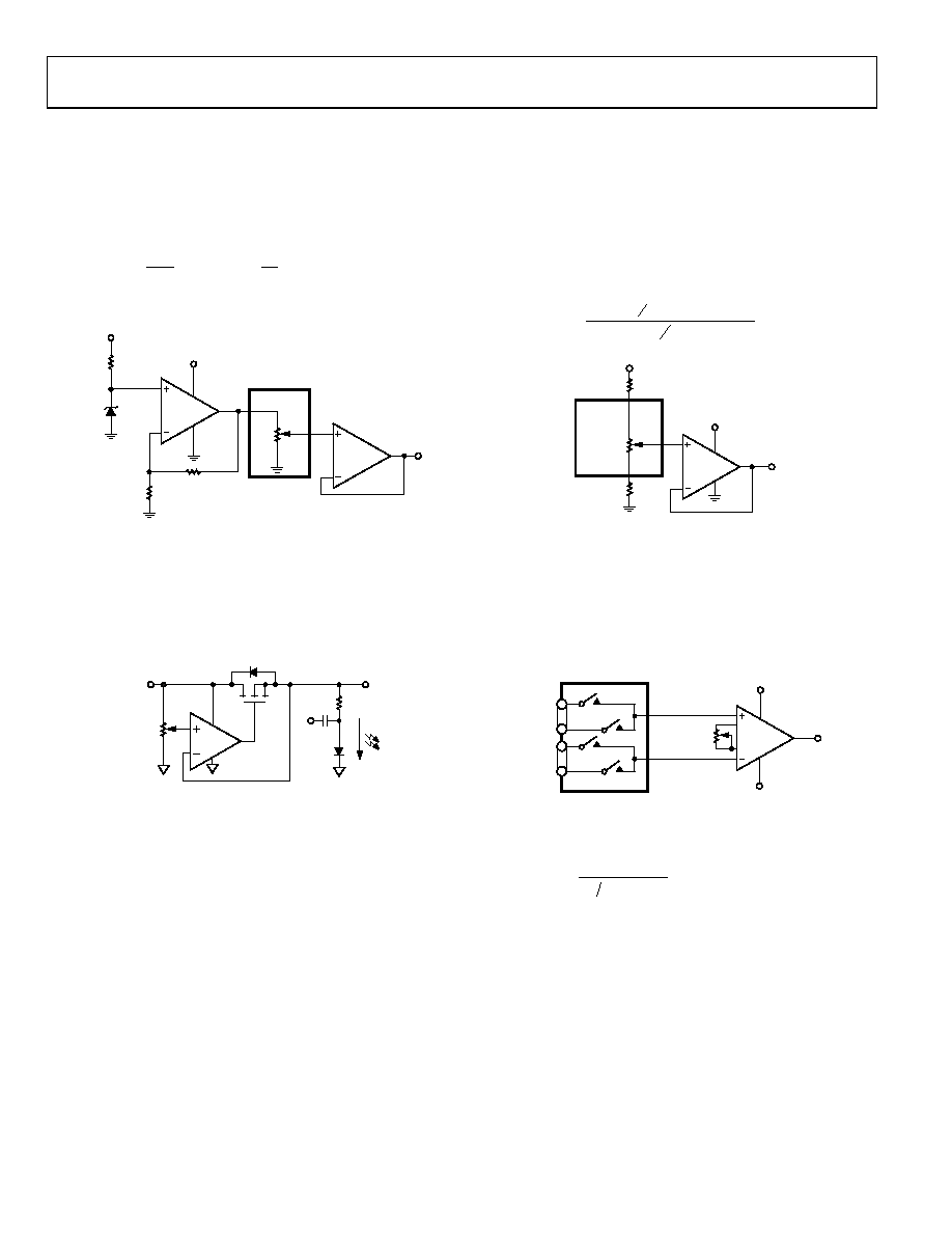
APPLICATIONS INFORMATION
HIGH VOLTAGE DAC
The AD5292 can be configured as a high voltage DAC, with
output voltage as high as 33 V. The circuit is shown in Figure 70.
The output is
+
×
=
1
2
1
V
2
.
1
1024
)
(
R
D
V
OUT
(7)
where D is the decimal code from 0 to 1023.
07
67
4-
1
53
AD5292
U2
AD8512
V+
V–
AD8512
VOUT
VDD
U1B
VDD
RBIAS
ADR512
D1
R2
R1
B
20k
U1A
Figure 70. High Voltage DAC
PROGRAMMABLE VOLTAGE SOURCE WITH
BOOSTED OUTPUT
For applications that require high current adjustments such as a
laser diode or tunable laser, a boosted voltage source can be
considered; see Figure 71.
07
67
4-
15
5
W
SIGNAL
CC
RBIAS
LD
VIN
A
B
VOUT
U1
AD5292
U3 2N7002
U2
IL
OP184
Figure 71. Programmable Boosted Voltage Source
In this circuit, the inverting input of the op amp forces VOUT to
be equal to the wiper voltage set by the digital potentiometer.
The load current is then delivered by the supply via the N-channel
FET (U3). The N-Channel FET power handling must be adequate
to dissipate (VIN VOUT) × IL power. This circuit can source a
maximum of 100 mA with a 33 V supply.
HIGH ACCURACY DAC
It is possible to configure the AD5292 as a high accuracy DAC
by optimizing the resolution of the device over a specific
reduced voltage range. This is achieved by placing external
resistors on either side of the RDAC, as shown in Figure 72.
The improved ±1% R-Tolerance specification greatly reduces
error associated with matching to discrete resistors.
3
1024
)
1024
(
1
1024
3
)
(
)
(
)
(
R
V
R
D
V
AB
D
DD
AB
D
OUT
+
×
+
×
+
=
(8)
07
67
4-
1
54
AD5292
U1
VOUT
B
R2
20k
R1
R3
±1%
OP1177
V+
V–
VDD
U2
Figure 72. Optimizing Resolution
VARIABLE GAIN INSTRUMENTATION AMPLIFIER
The AD8221 in conjunction with the AD5291 and AD5292 and
the ADG1207, as shown in Figure 73, make an excellent
instrumentation amplifier for use in data acquisition systems.
The data acquisition system’s low distortion and low noise
enable it to condition signals in front of a variety of ADCs.
07
67
4-
15
6
AD8221
AD5292
+VIN1
VDD
VOUT
VSS
ADG1207
+VIN4
–VIN1
–VIN4
Figure 73. Data Acquisition System
The gain can be calculated by using Equation 9.
()
AB
R
D
G
×
+
=
1024
kΩ
4
.
49
1
)
(
(9)
相关PDF资料 |
PDF描述 |
|---|---|
| VI-B3N-EW | CONVERTER MOD DC/DC 18.5V 100W |
| VI-B3K-EX | CONVERTER MOD DC/DC 40V 75W |
| VE-B6P-EX | CONVERTER MOD DC/DC 13.8V 75W |
| VE-B6P-EW | CONVERTER MOD DC/DC 13.8V 100W |
| H3AKH-2018G | IDC CABLE - HSC20H/AE20G/HPK20H |
相关代理商/技术参数 |
参数描述 |
|---|---|
| EVAL-AD5360EBZ | 功能描述:BOARD EVAL FOR AD5360 RoHS:是 类别:编程器,开发系统 >> 评估板 - 数模转换器 (DAC) 系列:- 产品培训模块:Lead (SnPb) Finish for COTS Obsolescence Mitigation Program 标准包装:1 系列:- DAC 的数量:4 位数:12 采样率(每秒):- 数据接口:串行,SPI? 设置时间:3µs DAC 型:电流/电压 工作温度:-40°C ~ 85°C 已供物品:板 已用 IC / 零件:MAX5581 |
| EVAL-AD5360EBZ1 | 制造商:AD 制造商全称:Analog Devices 功能描述:16-Channel, 16-/14-Bit, Serial Input, Voltage-Output DAC |
| EVAL-AD5361EBZ | 功能描述:BOARD EVAL FOR AD5361 RoHS:是 类别:编程器,开发系统 >> 评估板 - 数模转换器 (DAC) 系列:- 产品培训模块:Lead (SnPb) Finish for COTS Obsolescence Mitigation Program 标准包装:1 系列:- DAC 的数量:4 位数:12 采样率(每秒):- 数据接口:串行,SPI? 设置时间:3µs DAC 型:电流/电压 工作温度:-40°C ~ 85°C 已供物品:板 已用 IC / 零件:MAX5581 |
| EVAL-AD5361EBZ1 | 制造商:AD 制造商全称:Analog Devices 功能描述:16-Channel, 16-/14-Bit, Serial Input, Voltage-Output DAC |
| EVAL-AD5362EBZ | 功能描述:BOARD EVAL FOR AD5362 RoHS:是 类别:编程器,开发系统 >> 评估板 - 数模转换器 (DAC) 系列:- 产品培训模块:Lead (SnPb) Finish for COTS Obsolescence Mitigation Program 标准包装:1 系列:- DAC 的数量:4 位数:12 采样率(每秒):- 数据接口:串行,SPI? 设置时间:3µs DAC 型:电流/电压 工作温度:-40°C ~ 85°C 已供物品:板 已用 IC / 零件:MAX5581 |
发布紧急采购,3分钟左右您将得到回复。