- 您现在的位置:买卖IC网 > PDF目录17075 > EVAL-AD5371EBZ (Analog Devices Inc)BOARD EVAL FOR AD5371 PDF资料下载
参数资料
| 型号: | EVAL-AD5371EBZ |
| 厂商: | Analog Devices Inc |
| 文件页数: | 10/29页 |
| 文件大小: | 0K |
| 描述: | BOARD EVAL FOR AD5371 |
| 产品培训模块: | DAC Architectures |
| 标准包装: | 1 |
| DAC 的数量: | 40 |
| 位数: | 14 |
| 采样率(每秒): | 540k |
| 数据接口: | 串行 |
| 设置时间: | 20µs |
| DAC 型: | 电压 |
| 工作温度: | -40°C ~ 85°C |
| 已供物品: | 板,CD |
| 已用 IC / 零件: | AD5371 |
| 相关产品: | AD5371BSTZ-REEL-ND - IC DAC 14BIT 40CH SER 80-LQFP AD5371BBCZ-REELTR-ND - IC DAC 14BIT 40CH SER 100-CSPBGA |
第1页第2页第3页第4页第5页第6页第7页第8页第9页当前第10页第11页第12页第13页第14页第15页第16页第17页第18页第19页第20页第21页第22页第23页第24页第25页第26页第27页第28页第29页
AD5371
Rev. B | Page 17 of 28
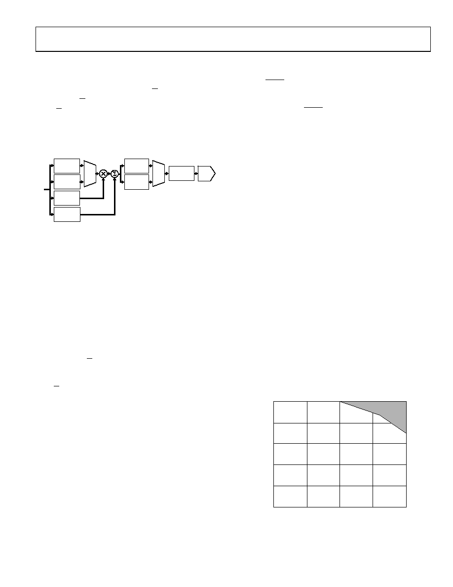
A/B REGISTERS AND GAIN/OFFSET ADJUSTMENT
Each DAC channel has seven data registers. The actual DAC
data-word can be written to either the X1A or the X1B input
register, depending on the setting of the A/B bit in the control
register. If the A/B bit is 0, data is written to the X1A register.
If the A/B bit is 1, data is written to the X1B register. Note that
this single bit is a global control and affects every DAC channel
in the device. It is not possible to set up the device on a per-
channel basis so that some writes are to X1A registers and
some writes are to X1B registers.
MUX
DAC
REGISTER
MUX
X1A
REGISTER
X1B
REGISTER
M
REGISTER
C
REGISTER
X2A
REGISTER
X2B
REGISTER
05
81
4-
02
0
Figure 20. Data Registers Associated with Each DAC Channel
Each DAC channel also has a gain (M) register and an offset (C)
register that allow trimming out of the gain and offset errors of
the entire signal chain. Data from the X1A register is operated
on by a digital multiplier and adder controlled by the contents of
the M and C registers. The calibrated DAC data is then stored in
the X2A register. Similarly, data from the X1B register is operated
on by the multiplier and adder and stored in the X2B register.
Although Figure 20 shows a multiplier and adder for each
channel, there is only one multiplier and one adder in the device
shared among all channels. This has implications for the update
speed when several channels are updated simultaneously, as
described in the Register Update Rates section.
Each time data is written to the X1A register, or to the M or C
register with the A/B control bit set to 0, the X2A data is recal-
culated and the X2A register is automatically updated. Similarly,
X2B is updated each time data is written to X1B, or to M or C
with A/B set to 1. The X2A and X2B registers are not readable
or directly writable by the user.
Data output from the X2A and X2B registers is routed to the
final DAC register by a multiplexer. Whether each individual
DAC takes its data from the X2A or X2B register is controlled
by an 8-bit A/B select register associated with each group of
eight DACs. If a bit in this register is 0, the DAC takes its data
from the X2A register; if 1, the DAC takes its data from the X2B
register (Bit 0 through Bit 7 control DAC 0 to DAC 7).
Note that because there are 40 bits in five registers, it is possible
to set up, on a per-channel basis, whether each DAC takes its
data from the X2A or X2B register. A global command is also
provided that sets all bits in the A/B select registers to 0 or to 1.
LOAD DAC
All DACs in the AD5371 can be updated simultaneously by
taking LDAC low when each DAC register is updated from
either its X2A or X2B register, depending on the setting of the
A/B select registers. The DAC register is not readable or directly
writable by the user. LDAC can be permanently tied low, and
the DAC output is updated whenever new data appears in the
appropriate DAC register.
OFFSET DACS
In addition to the gain and offset trim for each DAC, there are
three 14-bit offset DACs, one for Group 0, one for Group 1, and
one for Group 2 to Group 4. These allow the output range of all
DACs connected to them to be offset within a defined range.
Thus, subject to the limitations of headroom, it is possible to set
the output range of Group 0, Group 1, or Group 2 to Group 4 to
be unipolar positive, unipolar negative, or bipolar, either symmet-
rical or asymmetrical about 0 V. The DACs in the AD5371 are
factory trimmed with the offset DACs set at their default values.
This results in optimum offset and gain performance for the
default output range and span.
When the output range is adjusted by changing the value of the
offset DAC, an extra offset is introduced due to the gain error of
the offset DAC. The amount of offset is dependent on the magni-
tude of the reference and how much the offset DAC deviates from
its default value. See the Specifications section for this offset. The
worst-case offset occurs when the offset DAC is at positive or
negative full scale. This value can be added to the offset present
in the main DAC channel to give an indication of the overall
offset for that channel. In most cases, the offset can be removed
by programming the C register of the channel with an appropriate
value. The extra offset caused by the offset DAC needs to be taken
into account only when the offset DAC is changed from its default
value. Figure 21 shows the allowable code range that can be
loaded
to the offset DAC, depending on the reference value used.
Thus,
for a 5 V reference, the offset DAC should not be
programmed
with a value greater than 8192 (0x2000).
0
4096
8192
12288
16383
OFFSET DAC CODE
0
1
2
3
4
V
R
E
F
(V
)
5
RESERVED
05
81
4-
0
21
Figure 21. Offset DAC Code Range
相关PDF资料 |
PDF描述 |
|---|---|
| EMC05DRTF-S13 | CONN EDGECARD 10POS .100 EXTEND |
| SC53LC-470 | INDUCTOR SMD 47UH 0.62A 100KHZ |
| V375C2E50BF | CONVERTER MOD DC/DC 2V 50W |
| 101-1102 | KIT DEV RABBIT RCM4100 INTL |
| RCC17DRXN | CONN EDGECARD 34POS DIP .100 SLD |
相关代理商/技术参数 |
参数描述 |
|---|---|
| EVAL-AD5372EBZ | 功能描述:BOARD EVAL FOR AD5372 RoHS:是 类别:编程器,开发系统 >> 评估板 - 数模转换器 (DAC) 系列:- 产品培训模块:Lead (SnPb) Finish for COTS Obsolescence Mitigation Program 标准包装:1 系列:- DAC 的数量:4 位数:12 采样率(每秒):- 数据接口:串行,SPI? 设置时间:3µs DAC 型:电流/电压 工作温度:-40°C ~ 85°C 已供物品:板 已用 IC / 零件:MAX5581 |
| EVAL-AD5373EBZ | 功能描述:BOARD EVAL FOR AD5373 RoHS:是 类别:编程器,开发系统 >> 评估板 - 数模转换器 (DAC) 系列:- 产品培训模块:Lead (SnPb) Finish for COTS Obsolescence Mitigation Program 标准包装:1 系列:- DAC 的数量:4 位数:12 采样率(每秒):- 数据接口:串行,SPI? 设置时间:3µs DAC 型:电流/电压 工作温度:-40°C ~ 85°C 已供物品:板 已用 IC / 零件:MAX5581 |
| EVAL-AD5379EB | 制造商:AD 制造商全称:Analog Devices 功能描述:40-Channel, 14-Bit, Parallel and Serial Input, Bipolar Voltage-Output DAC |
| EVAL-AD5379EBZ | 功能描述:BOARD EVALUATION FOR AD5379 RoHS:是 类别:编程器,开发系统 >> 评估板 - 数模转换器 (DAC) 系列:- 产品培训模块:Lead (SnPb) Finish for COTS Obsolescence Mitigation Program 标准包装:1 系列:- DAC 的数量:4 位数:12 采样率(每秒):- 数据接口:串行,SPI? 设置时间:3µs DAC 型:电流/电压 工作温度:-40°C ~ 85°C 已供物品:板 已用 IC / 零件:MAX5581 |
| EVAL-AD5380EB | 制造商:Analog Devices 功能描述:EVALUATION BOARD I.C. - Bulk |
发布紧急采购,3分钟左右您将得到回复。