- 您现在的位置:买卖IC网 > PDF目录16569 > EVAL-AD5930EBZ (Analog Devices Inc)BOARD EVAL FOR AD5930 PDF资料下载
参数资料
| 型号: | EVAL-AD5930EBZ |
| 厂商: | Analog Devices Inc |
| 文件页数: | 9/28页 |
| 文件大小: | 0K |
| 描述: | BOARD EVAL FOR AD5930 |
| 标准包装: | 1 |
| 主要目的: | 计时,波形发生器 |
| 已用 IC / 零件: | AD5930 |
| 次要属性: | 串行接口 |
| 已供物品: | 板,线缆 |
第1页第2页第3页第4页第5页第6页第7页第8页当前第9页第10页第11页第12页第13页第14页第15页第16页第17页第18页第19页第20页第21页第22页第23页第24页第25页第26页第27页第28页
Data Sheet
AD5930
Rev. | Page 17 of 28
This is beneficial for applications where the user needs to burst
a frequency for a set period, and then “listen” for a response
before increasing to the next frequency. Note also that the
beginning of each frequency increment is at midscale (Phase 0
Rad). Therefore, the phase of the signal is always known.
To set up the AD5930 in burst mode, the CW/BURST bit (D7)
in the control register must be set to 1. See the Activating and
Controlling the Sweep section for more details about the burst
output mode.
SERIAL INTERFACE
The AD5930 has a standard 3-wire serial interface, which is
compatible with SPI, QSPI, MICROWIRE, and DSP
interface standards.
Data is loaded into the device as a 16-bit word under the
control of a serial clock input, SCLK. The timing diagram for
this operation is given in Figure 4.
The FSYNC input is a level-triggered input that acts as a frame
synchronization and chip enable. Data can only be transferred
into the device when FSYNC is low. To start the serial data
transfer, FSYNC should be taken low, observing the minimum
FSYNC to SCLK falling edge setup time, t7. After FSYNC goes
low, serial data is shifted into the device's input shift register on
the falling edges of SCLK for 16 clock pulses. FSYNC can be
taken high after the 16th falling edge of SCLK, observing the
minimum SCLK falling edge to FSYNC rising edge time, t8.
Alternatively, FSYNC can be kept low for a multiple of 16 SCLK
pulses, and then brought high at the end of the data transfer. In
this way, a continuous stream of 16-bit words can be loaded while
FSYNC is held low. FSYNC should only go high after the 16th
SCLK falling edge of the last word is loaded.
The SCLK can be continuous, or, alternatively, the SCLK can
idle high or low between write operations.
POWERING UP THE AD5930
When the AD5930 is powered up, the part is in an undefined
state, and therefore, must be reset before use. The eight registers
(control and frequency) contain invalid data and need to be set
to a known value by the user. The control register should be the
first register to be programmed, as this sets up the part. Note
that a write to the control register automatically resets the
internal state machines and provides an analog output of
midscale as it provides the same function as the INTERRUPT
pin. Typically, this is followed by a serial loading of all the
required sweep parameters. The DAC output remains at
midscale until a sweep is started using the CTRL pin.
PROGRAMMING THE AD5930
The AD5930 is designed to provide automatic frequency sweeps
when the CTRL pin is triggered. The automatic sweep is
controlled by a set of registers, the addresses of which are given
in Table 5. The function of each register is described in more
detail in the following section.
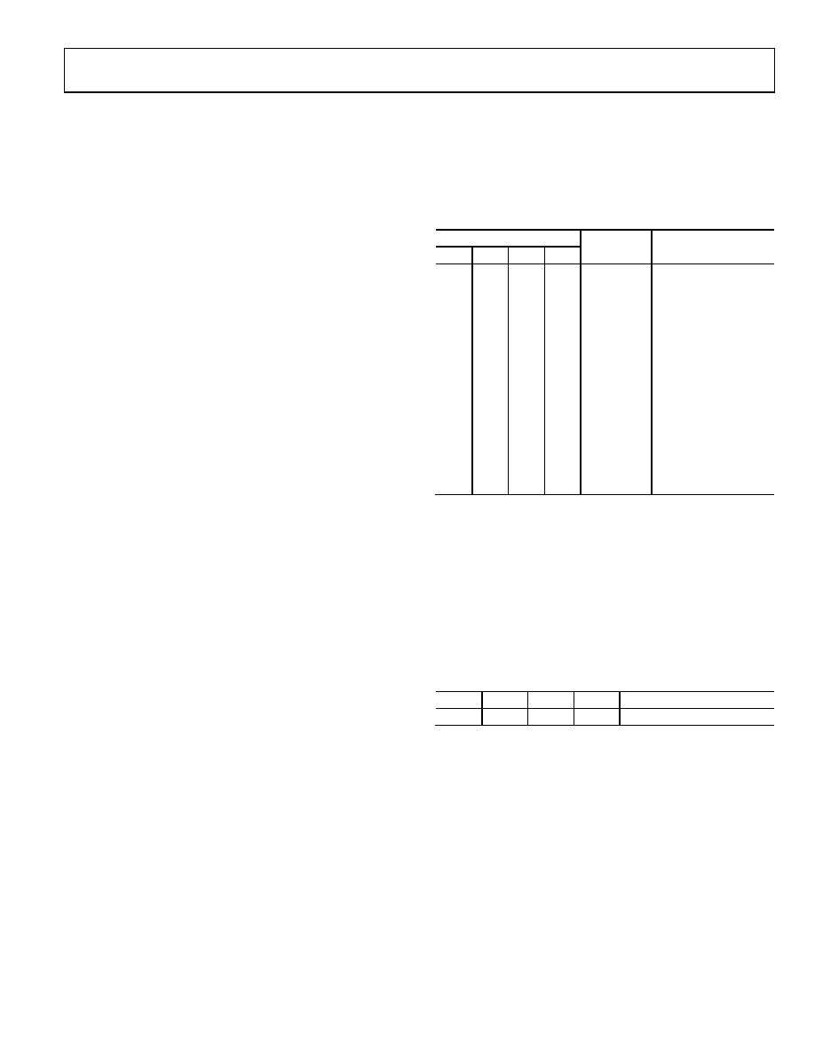
Table 5. Register Addresses
Register Address
D15
D14
D13
D12
Mnemonic
Name
0
CREG
Control bits
0
1
NINCR
Number of
increments
0
1
0
f
Lower 12 bits of delta
frequency
0
1
f
Higher 12 bits of
delta frequency
0
1
tINT
Increment interval
1
0
TBURST
Burst interval
1
0
FSTART
Lower 12 bits of start
frequency
1
0
1
FSTART
Higher 12 bits of start
frequency
1
0
Reserved
1
Reserved
The Control Register
The AD5930 contains a 12-bit control register (see Table 6) that
sets up the operating modes of the AD5930. The different
functions and the various output options from the AD5930 are
controlled by this register.
Table 7 describes the individual bits of the control register.
To address the control register, D15 to D12 of the 16-bit serial
word must be set to 0.
Table 6. Control Register
D15
D14
D13
D12
D11 to D0
0
Control Bits
B
相关PDF资料 |
PDF描述 |
|---|---|
| EBC31DCMI-S288 | CONN EDGECARD 62POS .100 EXTEND |
| A3DDB-1618G | IDC CABLE- AKR16B/AE16G/AKR16B |
| A1CXB-3436G | IDC CABLE- AKC34B/AE34G/X |
| GCM18DTBI | CONN EDGECARD 36POS R/A .156 SLD |
| H3CKH-1436G | IDC CABLE - HKC14H/AE14G/HPK14H |
相关代理商/技术参数 |
参数描述 |
|---|---|
| EVAL-AD5932EB | 制造商:Analog Devices 功能描述:EVALUATION BOARD - Bulk |
| EVAL-AD5932EBZ | 功能描述:BOARD EVAL FOR AD5932 RoHS:是 类别:编程器,开发系统 >> 评估演示板和套件 系列:- 标准包装:1 系列:- 主要目的:电信,线路接口单元(LIU) 嵌入式:- 已用 IC / 零件:IDT82V2081 主要属性:T1/J1/E1 LIU 次要属性:- 已供物品:板,电源,线缆,CD 其它名称:82EBV2081 |
| EVALAD5933EB | 制造商:AD 制造商全称:Analog Devices 功能描述:Evaluation Board for the 1 MSPS 12-Bit Impedance Converter Network Analyzer |
| EVAL-AD5933EB | 制造商:Analog Devices 功能描述:EVALUATION BOARD I.C. - Bulk |
| EVAL-AD5933EB-U1 | 制造商:Analog Devices 功能描述:- Bulk |
发布紧急采购,3分钟左右您将得到回复。