- 您现在的位置:买卖IC网 > PDF目录17048 > EVAL-AD7194EBZ (Analog Devices Inc)EVAL BOARD FOR AD7194 PDF资料下载
参数资料
| 型号: | EVAL-AD7194EBZ |
| 厂商: | Analog Devices Inc |
| 文件页数: | 26/57页 |
| 文件大小: | 0K |
| 描述: | EVAL BOARD FOR AD7194 |
| 设计资源: | EVAL-AD7zzzEBZ Schematic AD7194 Gerber Files |
| 标准包装: | 1 |
| ADC 的数量: | 1 |
| 位数: | 24 |
| 数据接口: | DSP,MICROWIRE?,QSPI?,串行,SPI? |
| 工作温度: | -40°C ~ 105°C |
| 已用 IC / 零件: | AD7194 |
| 已供物品: | 板,线缆 |
第1页第2页第3页第4页第5页第6页第7页第8页第9页第10页第11页第12页第13页第14页第15页第16页第17页第18页第19页第20页第21页第22页第23页第24页第25页当前第26页第27页第28页第29页第30页第31页第32页第33页第34页第35页第36页第37页第38页第39页第40页第41页第42页第43页第44页第45页第46页第47页第48页第49页第50页第51页第52页第53页第54页第55页第56页第57页
Data Sheet
AD7194
Rev. A | Page 31 of 56
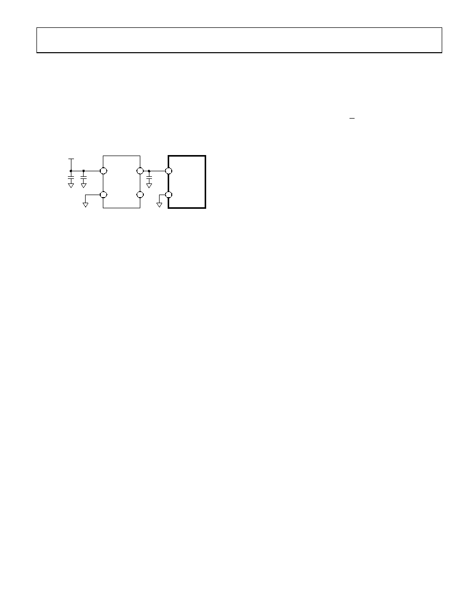
impedance. External decoupling on the REFINx pins is not
recommended in this type of circuit configuration. Conversely,
if large decoupling capacitors are used on the reference inputs,
there should be no resistors in series with the reference inputs.
Recommended 2.5 V reference voltage sources for the AD7194
include the ADR421 and ADR431, which are low noise references.
These references tolerate decoupling capacitors on REFINx(+)
without introducing gain errors in the system. Figure 23 shows the
recommended connections between the ADR421 and the AD7194.
4
2
0.1F
AVDD
ADR421
AD7194
VIN
GND
REFINx(+)
REFINx(–)
VOUT
TRIM
10F
4.7F
6
5
08566-
022
Figure 23. ADR421 to AD7194 Connections
REFERENCE DETECT
The AD7194 includes on-chip circuitry to detect whether the
part has a valid reference for conversions or calibrations. This
feature is enabled when the REFDET bit in the configuration
register is set to 1. If the voltage between the selected REFINx(+)
and REFINx() pins is less than 0.3 V, the AD7194 detects that
it no longer has a valid reference. In this case, the NOREF bit
of the status register is set to 1. When the voltage between the
selected REFINx(+) and REFINx() pins is greater than 0.6 V,
the AD7194 detects a valid reference; thus, the NOREF bit is set
to 0. The operation of the NOREF bit is undefined when the
voltage between the selected REFINx(+) and REFINx() pins
is between 0.3 V and 0.6 V.
If the AD7194 is performing normal conversions and the
NOREF bit becomes active, the conversion result is all 1s.
Therefore, it is not necessary to continuously monitor the
status of the NOREF bit when performing conversions. It is
only necessary to verify its status if the conversion result read
from the ADC data register is all 1s.
If the AD7194 is performing either an offset or full-scale cali-
bration and the NOREF bit becomes active, the updating of the
respective calibration registers is inhibited to avoid loading
incorrect coefficients to these registers, and the ERR bit in the
status register is set. If the user is concerned about verifying that
a valid reference is in place every time a calibration is performed,
the status of the ERR bit should be checked at the end of the
calibration cycle.
BIPOLAR/UNIPOLAR CONFIGURATION
The analog input to the AD7194 can accept either unipolar or
bipolar input voltage ranges. A bipolar input range does not
imply that the part can tolerate negative voltages with respect
to system AGND. In pseudo differential mode, signals are
referenced to AINCOM, whereas in differential mode, signals
are referenced to the negative input of the differential pair. For
example, if AINCOM is 2.5 V and the AD7194 AIN1 analog
input is configured for unipolar mode with a gain of 2, the input
voltage range on the AIN1 pin is 2.5 V to 3.75 V when a 2.5 V
reference is used.
If AINCOM is 2.5 V and the AD7194 AIN1 analog input is
configured for bipolar mode with a gain of 2, the analog input
range on AIN1 is 1.25 V to 3.75 V. The bipolar/unipolar option
is chosen by programming the U/B bit in the configuration
register.
DATA OUTPUT CODING
When the ADC is configured for unipolar operation, the output
code is natural (straight) binary with a zero differential input
voltage resulting in a code of 00...00, a midscale voltage resulting
in a code of 100...000, and a full-scale input voltage resulting in
a code of 111...111. The output code for any analog input
voltage can be represented as
Code = (2N × AIN × Gain)/VREF
When the ADC is configured for bipolar operation, the output
code is offset binary with a negative full-scale voltage resulting
in a code of 000...000, a zero differential input voltage resulting
in a code of 100...000, and a positive full-scale input voltage
resulting in a code of 111...111. The output code for any analog
input voltage can be represented as
Code = 2(N–1) × [(AIN × Gain/VREF) + 1]
where:
AIN is the analog input voltage.
Gain is the PGA setting (1 to 128).
N = 24.
BURNOUT CURRENTS
The AD7194 contains two 500 nA constant current generators,
one sourcing current from AVDD to AIN(+) and one sinking
current from AIN() to AGND. The currents are switched to
the selected analog input pair. Both currents are either on or off,
depending on the burnout current enable (burn) bit in the
configuration register.
These currents can be used to verify that an external transducer
remains operational before attempting to take measurements on
that channel. After the burnout currents are turned on, they flow in
the external transducer circuit, and a measurement of the input
voltage on the analog input channel can be taken. It takes some
time for the burnout currents to detect an open circuit condition
because the currents must charge any external capacitors.
There are several reasons that a fault condition is detected: the
front-end sensor may be either open circuit or overloaded, or
the reference may be absent and the NOREF bit in the status
register is set, thus clamping the data to all 1s. The user must
check these three cases before making a determination.
If the voltage measured is 0 V, it may indicate that the transducer
has short circuited. The current sources work over the normal
absolute input voltage range specifications when the analog
inputs are buffered and chop is disabled.
相关PDF资料 |
PDF描述 |
|---|---|
| ECC22DCMT-S288 | CONN EDGECARD 44POS .100 EXTEND |
| 0210490257 | CABLE JUMPER 1.25MM .051M 20POS |
| ADR445ARMZ-REEL7 | IC VREF SERIES PREC 5V 8-MSOP |
| RBC19DRYN-S13 | CONN EDGECARD 38POS .100 EXTEND |
| HKQ0603S0N7C-T | INDUCTOR HI FREQ 0.7NH 0201 |
相关代理商/技术参数 |
参数描述 |
|---|---|
| EVAL-AD7195EBZ | 功能描述:BOARD EVAL FOR AD7195 RoHS:是 类别:编程器,开发系统 >> 评估演示板和套件 系列:- 标准包装:1 系列:- 主要目的:电信,线路接口单元(LIU) 嵌入式:- 已用 IC / 零件:IDT82V2081 主要属性:T1/J1/E1 LIU 次要属性:- 已供物品:板,电源,线缆,CD 其它名称:82EBV2081 |
| EVAL-AD7262EDZ | 功能描述:BOARD EVAL CONTROL AD7262 RoHS:是 类别:编程器,开发系统 >> 评估板 - 模数转换器 (ADC) 系列:- 产品培训模块:Obsolescence Mitigation Program 标准包装:1 系列:- ADC 的数量:1 位数:12 采样率(每秒):94.4k 数据接口:USB 输入范围:±VREF/2 在以下条件下的电源(标准):- 工作温度:-40°C ~ 85°C 已用 IC / 零件:MAX11645 已供物品:板,软件 |
| EVAL-AD7264EDZ | 功能描述:BOARD EVALUATION FOR AD7264 RoHS:是 类别:编程器,开发系统 >> 评估板 - 模数转换器 (ADC) 系列:- 产品培训模块:Obsolescence Mitigation Program 标准包装:1 系列:- ADC 的数量:1 位数:12 采样率(每秒):94.4k 数据接口:USB 输入范围:±VREF/2 在以下条件下的电源(标准):- 工作温度:-40°C ~ 85°C 已用 IC / 零件:MAX11645 已供物品:板,软件 |
| EVAL-AD7265CB | 制造商:AD 制造商全称:Analog Devices 功能描述:Differential/Single-Ended Input, Dual 1 MSPS, 12-Bit, 3-Channel SAR ADC |
| EVAL-AD7265CB1 | 制造商:AD 制造商全称:Analog Devices 功能描述:Differential Input, Dual 1 MSPS, 12-Bit, 3-Channel SAR ADC |
发布紧急采购,3分钟左右您将得到回复。