- 您现在的位置:买卖IC网 > PDF目录17048 > EVAL-AD7194EBZ (Analog Devices Inc)EVAL BOARD FOR AD7194 PDF资料下载
参数资料
| 型号: | EVAL-AD7194EBZ |
| 厂商: | Analog Devices Inc |
| 文件页数: | 37/57页 |
| 文件大小: | 0K |
| 描述: | EVAL BOARD FOR AD7194 |
| 设计资源: | EVAL-AD7zzzEBZ Schematic AD7194 Gerber Files |
| 标准包装: | 1 |
| ADC 的数量: | 1 |
| 位数: | 24 |
| 数据接口: | DSP,MICROWIRE?,QSPI?,串行,SPI? |
| 工作温度: | -40°C ~ 105°C |
| 已用 IC / 零件: | AD7194 |
| 已供物品: | 板,线缆 |
第1页第2页第3页第4页第5页第6页第7页第8页第9页第10页第11页第12页第13页第14页第15页第16页第17页第18页第19页第20页第21页第22页第23页第24页第25页第26页第27页第28页第29页第30页第31页第32页第33页第34页第35页第36页当前第37页第38页第39页第40页第41页第42页第43页第44页第45页第46页第47页第48页第49页第50页第51页第52页第53页第54页第55页第56页第57页
Data Sheet
AD7194
Rev. A | Page 41 of 56
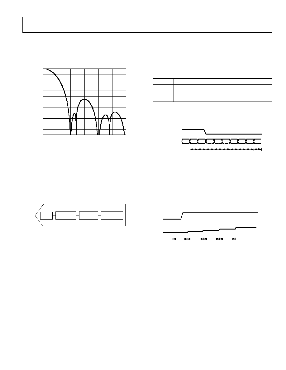
The output data rate is 50 Hz when zero latency is disabled and
12.5 Hz when zero latency is enabled. Figure 34 shows the
frequency response of the sinc4 filter. The filter provides 50 Hz
±1 Hz and 60 Hz ± 1 Hz rejection of 82 dB minimum, assuming
a stable 4.92 MHz master clock.
–120
–110
–100
–90
–80
–70
–60
–50
–40
–30
–20
–10
0
25
50
75
100
125
150
FREQUENCY (Hz)
FI
L
T
E
R
G
AI
N
(
d
B)
08566-
033
Figure 34. Sinc4 Filter Response (FS[9:0] = 96, REJ60 = 1)
SINC3 FILTER (CHOP DISABLED)
A sinc3 filter can be used instead of the sinc4 filter. The filter is
selected using the SINC3 bit in the mode register. The sinc3
filter is selected when the SINC3 bit is set to 1.
This filter has good noise performance when operating with
output data rates up to 1 kHz. It has moderate settling time and
moderate 50 Hz/60 Hz (±1 Hz) rejection.
SINC3/SINC4
POST FILTER
MODULATOR
ADC
CHOP
08566-
034
Figure 35. Sinc3 Filter (Chop Disabled)
Sinc3 Output Data Rate and Settling Time
The output data rate (the rate at which conversions are available
on a single channel when the ADC is continuously converting)
is equal to
fADC = fCLK/(1024 × FS[9:0])
where:
fADC is the output data rate.
fCLK is the master clock (4.92 MHz nominal).
FS[9:0] is the decimal equivalent of Bit FS9 to Bit FS0 in the
mode register.
The output data rate can be programmed from 4.7 Hz to
4800 Hz; that is, FS[9:0] can have a value from 1 to 1023.
The settling time is equal to
tSETTLE = 3/fADC
The 3 dB frequency is equal to
f3dB = 0.272 × fADC
Table 30 gives some examples of FS settings and the corres-
ponding output data rates and settling times.
Table 30. Examples of Output Data Rates and the
Corresponding Settling Time
FS[9:0]
Output Data Rate (Hz)
Settling Time (ms)
480
10
300
96
50
60
80
60
50
When a channel change occurs, the modulator and filter reset.
The complete settling time is allowed to generate the first
conversion after the channel change (see Figure 36). Subsequent
conversions on this channel are available at 1/fADC.
CHANNEL
CONVERSIONS
CHANNEL A
CH A
CH B
CHANNEL B
1/
fADC
08566-
035
Figure 36. Sinc3 Channel Change
When conversions are performed on a single channel and a step
change occurs, the ADC does not detect the change in analog
input. Therefore, it continues to output conversions at the
programmed output data rate. However, it is at least three
conversions later before the output data accurately reflects the
analog input. If the step change occurs while the ADC is
processing a conversion, the ADC takes four conversions after
the step change to generate a fully settled result.
1/
fADC
ANALOG
INPUT
ADC
OUTPUT
FULLY
SETTLED
08566-
036
Figure 37. Asynchronous Step Change in Analog Input
Sinc3 Zero Latency
Zero latency is enabled by setting the single bit (Bit 11) in the
mode register to 1. With zero latency, the complete settling time
is allowed for each conversion. Therefore, the conversion time
when converting on a single channel or when converting on
several channels is constant. The user does not need to consider
the effects of channel changes on the output data rate.
相关PDF资料 |
PDF描述 |
|---|---|
| ECC22DCMT-S288 | CONN EDGECARD 44POS .100 EXTEND |
| 0210490257 | CABLE JUMPER 1.25MM .051M 20POS |
| ADR445ARMZ-REEL7 | IC VREF SERIES PREC 5V 8-MSOP |
| RBC19DRYN-S13 | CONN EDGECARD 38POS .100 EXTEND |
| HKQ0603S0N7C-T | INDUCTOR HI FREQ 0.7NH 0201 |
相关代理商/技术参数 |
参数描述 |
|---|---|
| EVAL-AD7195EBZ | 功能描述:BOARD EVAL FOR AD7195 RoHS:是 类别:编程器,开发系统 >> 评估演示板和套件 系列:- 标准包装:1 系列:- 主要目的:电信,线路接口单元(LIU) 嵌入式:- 已用 IC / 零件:IDT82V2081 主要属性:T1/J1/E1 LIU 次要属性:- 已供物品:板,电源,线缆,CD 其它名称:82EBV2081 |
| EVAL-AD7262EDZ | 功能描述:BOARD EVAL CONTROL AD7262 RoHS:是 类别:编程器,开发系统 >> 评估板 - 模数转换器 (ADC) 系列:- 产品培训模块:Obsolescence Mitigation Program 标准包装:1 系列:- ADC 的数量:1 位数:12 采样率(每秒):94.4k 数据接口:USB 输入范围:±VREF/2 在以下条件下的电源(标准):- 工作温度:-40°C ~ 85°C 已用 IC / 零件:MAX11645 已供物品:板,软件 |
| EVAL-AD7264EDZ | 功能描述:BOARD EVALUATION FOR AD7264 RoHS:是 类别:编程器,开发系统 >> 评估板 - 模数转换器 (ADC) 系列:- 产品培训模块:Obsolescence Mitigation Program 标准包装:1 系列:- ADC 的数量:1 位数:12 采样率(每秒):94.4k 数据接口:USB 输入范围:±VREF/2 在以下条件下的电源(标准):- 工作温度:-40°C ~ 85°C 已用 IC / 零件:MAX11645 已供物品:板,软件 |
| EVAL-AD7265CB | 制造商:AD 制造商全称:Analog Devices 功能描述:Differential/Single-Ended Input, Dual 1 MSPS, 12-Bit, 3-Channel SAR ADC |
| EVAL-AD7265CB1 | 制造商:AD 制造商全称:Analog Devices 功能描述:Differential Input, Dual 1 MSPS, 12-Bit, 3-Channel SAR ADC |
发布紧急采购,3分钟左右您将得到回复。